원자력공학과, ‘원자력 안전규제라운드테이블’ 개최

연구 2026년 07월 15일 수요일

"부정맥부터 가스 위험 감지까지"… 패치 안에서 바로 판단하는 온칩 AI 기술 개발

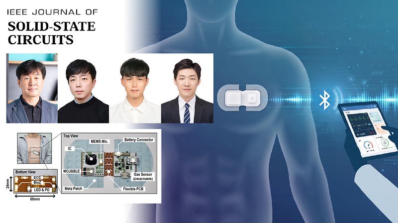
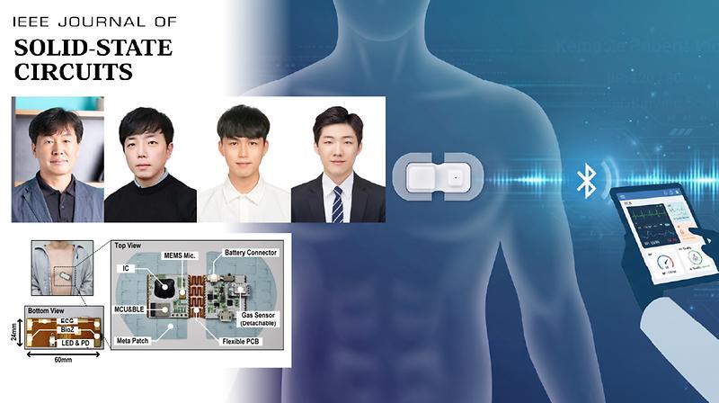
심전도, 혈압과 같은 생체 신호와 대기 가스 정보를 동시에 분석해 질병이나 위험 상황을 알 수 있는 부착형 패치가 개발됐다. 대기오염에 민감한 기저질환자, 노약자의 맞춤형 건강관리나, 밀폐 공간 작업자 모니터링에 쓸 수 있는 기술이다. UNIST 전기전자공학과 김재준 교수팀과 기계공학과 정훈의 교수팀은 심전도, 혈압과 같은 생체 정보와 함께 주변 유해 가스를 동시에 감지해 심혈관 질병이나 이상 상태를 즉시 판별할 수 있는 가슴 부착형 패치를 개발했다고 30일 밝혔다. 이 패치는 아날로그 연산 기반 온칩 인공지능 회로를 이용해 센서가 측정한 측정 데이터를 외부로 보내지 않고 패치 내부에서 바로 분석해 낸다. 판단 결과를 블루투스를 통해 외부로 전송할 수 있어, 관리자가 여러 명을 동시에 원격으로 모니터링할 수 있다. 무거운 원시 데이터(Raw data) 대신 칩이 자체 판단한 가벼운 결괏값만 전송하므로 통신 끊김과 지연은 최소화하고, 통신 자체에 드는 전력 소모를 줄였다. 또 광학 센서를 선택적으로 작동시키는 저전력 회로 설계 기술이 적용돼 한 번 충전으로 장시간 착용할 수 있다. 광학 센서는 혈류 정보를 얻는 역할을 하는데, 기기에서 전력 소모가 가장 많다. 연구진은 심전도 신호 주기에 맞춰 센서를 켜고 끄는 저전력 기술(RPT-PW)을 적용한 결과, 기존 대비 해당 센서부의 전력 소모가 약 83%나 줄었다. 개발된 패치는 고혈압이나 부정맥을 90% 이상의 정확도로 진단했으며, 유해가스 혼합물 분류 실험에서, 92.46%의 진단 정확도를 기록했다. 패치 접착면에 미세 구조 기술이 적용돼, 거친 피부에도 잘 접착되며, 패치를 떼어낼 때는 한쪽 방향으로 쉽게 떨어져 잔여물이 남지 않는다. UNIST 전기전자공학과 조상현 연구원과 김현중 연구원이 제1저자로 참여한 이번 연구는 회로 설계 분야 최고 학술지인 ‘IEEE 저널 오브 솔리드 스테이트 서킷스(Journal of Solid-State Circuits)’ 7월호에 정식 게재될 예정이다. 한편 연구진이 공동 창업한 ㈜앤빅스랩(Anvix Lab)은 개발된 기술을 이전받아 온칩 AI 기반의 차세대 바이오일렉트로넥스 패치 플랫폼 상용화를 추진 중이다. 이번 연구는 산업통상부, 교육부, 과학기술정보통신부의 지원을 받아 수행되었다.

원자력공학과, ‘원자력 안전규제라운드테이블’ 개최

연구 2026년 07월 01일 수요일

우주·6G 통신 칩 전력 줄일 반도체 소자 개발

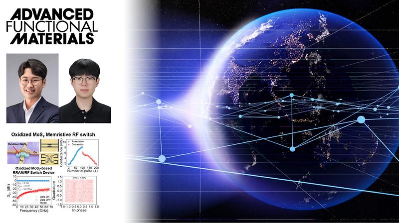
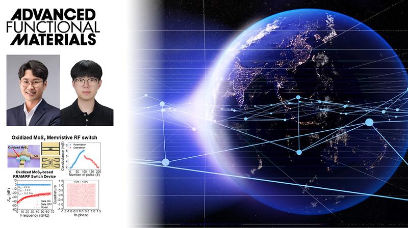
전력과 공간 제약이 큰 우주 위성통신과 6G 통신에서 데이터를 더 적은 전력으로 처리할 수 있는 반도체 소자가 개발됐다. UNIST 전기전자공학과 김명수 교수팀은 산화 2차원 반도체 소재를 기반으로 한 다기능 멤리스터 반도체 소자를 개발했다고 22일 밝혔다. 이 멤리스터 반도체 소자는 통신 고주파 신호의 길을 여닫는 RF 스위치와 연산 소자로 모두 쓸 수 있다. 덕분에 칩 면적을 작게 만들 수 있고, 신호를 다른 회로로 옮기고 변환하는 과정에서 드는 전력과 지연도 낮출 수 있다. 또 한 번 상태를 바꿔 두면 전원을 끊어도 켜짐·꺼짐 상태가 유지돼, 대기 전력 소모가 없다. 태양광 등 제한된 에너지만으로 작동해야 하는 위성 통신 장비나 6G 기지국처럼 전력과 공간 제약이 극심한 시스템에 이 기술이 적합한 이유다. 연구팀은 2차원 반도체 소재인 이황화몰리브덴(MoS2)을 400℃에서 산화시켜 이 같은 소자를 만들었다. 산화 이황화몰리브덴은 전압을 걸었을 때 저항이 낮아져 스위치가 켜지고, 전압을 반대 방향으로 걸면 저항이 높아져 스위치가 꺼지게 된다. 별도로 전압을 걸어주지 않는 한 저항 상태가 유지되기 때문에 대기 전력이 필요 없게 된다. 이 단일 소자를 바둑판처럼 배열한 회로로는 연산을 할 수 있다. 각 소자의 저항(전도도)이 행렬 계산에서 가중치 역할을 할 수 있기 때문이다. 통신에서는 여러 안테나에서 들어온 신호가 서로 섞여 있어서 원하는 신호를 골라내려면 각 신호에 알맞은 비율을 곱해 더하는 행렬 연산이 필요하다. 기존에는 이 계산을 위해 아날로그 고주파 신호를 디지털 신호로 바꾸고, 별도의 프로세서 회로로 데이터를 옮겨 처리해야 했다. 실험에서 이 소자를 한 번 켜거나 끄는 데 드는 스위칭 에너지는 140pJ(피코줄, 10⁻12)로 매우 낮았고, 상태를 바꾸는 동작 전력 역시 1mW(밀리와트) 이하로 측정됐다. 한 번 바뀐 저항 상태는 4만 초 이상 유지되는 비휘발성과 1,000회 이상 반복 동작에서도 안정성을 보였다. 초고속 통신에 쓰이는 고주파 대역의 스위칭 성능은 실험에서 67GHz까지 검증됐다. ON 저항과 OFF 커패시턴스를 기반으로 계산한 차단주파수는 33.2THz에 달했다. 연구팀은 소자 회로의 연산 성능도 시뮬레이션으로 검증해, 1024-QAM 신호 복조와 MIMO 신호 복원이 이뤄짐을 확인했다. 제1저자인 손주호 연구원은 “기존 상용 반도체 고주파 스위치는 지속해서 대기 전력을 소모하고 고주파 대역에서 신호 손실이 발생하는 문제가 있었는데, 이 소자는 이러한 한계를 근본적으로 해결한 기술”이라며 “차세대 상변화 메모리(PCM)나 MEMS와 비교해도 각각 에너지 소모 효율과 초고주파 동작 속도 및 초소형화 측면에서 경쟁력을 갖춘 기술”이라고 설명했다. 김명수 교수는 “이번 연구는 산화 2차원 반도체 기반 멤리스터가 고성능 밀리미터파 RF 스위치뿐 아니라 6G 신호처리에 필요한 인메모리 행렬 연산 하드웨어로도 활용될 수 있음을 보여준 사례”라며, “비휘발성·저전력·고주파 특성을 동시에 확보한 만큼, 위성통신, 레이더, 방산용 전파 제어 시스템, 6G RF 프론트엔드의 소형화와 에너지 효율 향상에 기여할 수 있을 것”이라고 설명했다. 이번 연구는 과학기술정보통신부 한국연구재단, 정보통신기획평가원의 우수신진연구, Space-K BIG 프로젝트, 지역지능화혁신인재양성사업의 지원을 받아 수행됐으며, 연구 결과는 세계적 학술지 ‘어드밴스드 펑셔널 머티리얼즈(Advanced Functional Materials)’에 6월 6일 온라인 공개됐다. (끝)

원자력공학과, ‘원자력 안전규제라운드테이블’ 개최

대학소식 2026년 06월 09일 화요일

UNIST 전기전자공학과, 우주항공청 ‘Space-K BIG 프로젝트’ 선정

UNIST 전기전자공학과 연구팀이 우주항공청(KASA)이 주관하는 ‘2026년도 Space-K BIG 프로젝트 사업’ 인공위성·우주임무보증 분야 신규 과제 수행 기관으로 최종 선정됐다. Space-K BIG 프로젝트는 우주 분야 기술개발 역량과 인력양성 기반을 갖춘 대학을 연구센터로 지정해 기초·원천기술을 축적하고, 전문 인재를 체계적으로 길러내는 우주항공청의 핵심 사업이다. 이번 선정으로 UNIST 연구팀은 2030년 12월까지 연구를 수행한다. 총 57억 원의 정부출연금을 지원받아 임무 주도형 초저궤도 위성 플랫폼 개발과 우주 특화 인재 양성에 속도를 낸다. 이번 대형 과제는 전기전자공학과 변강일 교수가 연구책임자를 맡았다. 김명수, 이훈, 박진석, 최민호, 감동윤, 한가원, 정재용 교수가 함께 참여해 학과의 연구 역량을 모은다. 선정된 연구개발과제는 ‘임무 주도형 초저궤도 위성 융복합 플랫폼 원천기술 확보 및 글로벌 인재 양성’이다. 연구팀은 우주 임무에 필요한 핵심 소자와 부품, 플랫폼 기술을 아우르는 융복합 연구를 추진한다. 주요 연구 방향은 세 가지다. 먼저 RF, AI 반도체, 광·전자 소자가 극한 우주 환경에서도 안정적으로 작동할 수 있도록 신뢰성을 확보한다. 이어 저궤도 위성에 적용할 수 있는 국산 COTS, 즉 상용 완제품을 개발하고, 실제 운용을 통해 우주 헤리티지 확보에 나선다. 또 초저궤도 위성 융합 플랫폼을 구축해 미래 우주 임무에 투입할 수 있는 실전형 기술 기반을 마련한다. 인재 양성도 핵심 축이다. UNIST 연구팀은 국내외 우주항공 분야 기업, 정부출연연구소와 산·학·연 협력 생태계를 꾸려 공동 연구를 수행할 계획이다. 실습과 공동 프로젝트를 연계한 교육 프로그램을 운영해 연구개발과 교육이 맞물려 돌아가는 선순환 체계도 구축한다. 연구책임자 변강일 교수는 “이번 Space-K BIG 프로젝트 선정을 계기로 UNIST가 대한민국 초저궤도 위성 원천기술 연구를 선도하고, 세계적 수준의 우주 특화 인재를 배출할 기반을 마련했다”며 “참여 교수진의 전문성과 협력 기업의 혁신 기술을 결합해 미래 우주 산업에 실질적으로 기여할 성과를 내겠다”고 말했다.

원자력공학과, ‘원자력 안전규제라운드테이블’ 개최

커뮤니티 2026년 06월 05일 금요일

윤성환 교수, ‘디지털인재양성 공로’ 과기정통부 장관 표창

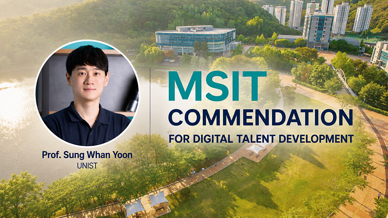
윤성환 교수(인공지능대학원·전기전자공학과)가 디지털인재양성 공로로 부총리 겸 과학기술정보통신부 장관 표창을 수상했다. AI 기술을 제조 현장 교육과 공정 혁신으로 연결해 온 점을 인정받았다. AI를 공장에 적용할 때 가장 큰 변수는 현장이다. 연구실에서 학습한 데이터와 실제 설비에서 들어오는 데이터는 같지 않다. 원료 상태, 장비 조건, 운전 방식, 데이터 품질이 바뀌면 모델의 판단도 흔들릴 수 있다. 제조업에서는 이런 오류가 곧 생산 손실이나 안전 문제로 이어진다. 윤 교수는 이런 한계를 줄이는 ‘강건한 인공지능’ 학습 알고리즘을 개발해 왔다. 강건한 AI는 학습 때 보지 못한 환경 변화가 생겨도 안정적으로 작동하는 기술이다. 정해진 조건에서 높은 정확도를 내는 데 그치지 않고, 실제 산업 현장에서 신뢰할 수 있는 판단을 내리도록 만드는 것이 핵심이다. 그의 연구 역량은 딥러닝 분야 대표 학술대회인 ‘International Conference on Learning Representations(ICLR 2025)’에서 높이 평가됐다. 윤 교수는 AI 기반 최적화 기술인 강화학습 모델의 안정성을 높인 연구로 구두 발표 논문에 선정됐다. ICLR 구두 발표는 제출 논문 가운데 상위 2% 수준의 연구에 주어지는 성과다. 강화학습은 AI가 여러 선택을 시도하고 결과를 학습해 더 나은 결정을 찾아가는 기술이다. 제조 현장에서는 설비 운전 조건을 조정하거나 생산 공정을 효율화하는 데 활용될 수 있다. 다만 공장에서는 한 번의 잘못된 결정도 비용과 안전 리스크로 이어질 수 있다. 윤 교수의 연구는 강화학습이 불확실한 현장 조건에서도 흔들리지 않도록 신뢰성을 높였다는 점에서 주목받았다. 논문으로 검증한 기술은 울산과 동남권 제조업 교육 현장으로도 옮겨졌다. 윤 교수는 UNIST 부임 이후 산업체 재직자 대상 AI 교육 설계와 운영에 참여했다. 교육은 이론 강의가 아니라 현장 문제 해결에 맞춰졌다. 재직자들이 공정에서 겪는 문제를 제시하고, 이를 AI 실습 과제로 바꾸는 방식이었다. 공장 단위 생산·가공 설비에 강화학습 기반 최적화 기법을 적용한 사례도 만들었다. 공정의 안전성과 안정성을 유지하면서 설비 운영을 개선하는 접근이다. AI를 배우는 데서 끝내지 않고 실제 업무 변화로 이어지게 한 점이 이번 표창의 주요 배경으로 꼽힌다. 그는 현재 UNIST가 수행 중인 국가 주요 AI 연구 과제인 ‘AI스타펠로우십’에서 신진 프로젝트 리더로도 참여하고 있다. SK에너지와 협력해 석유화학 산업을 포함한 공정 프로세스에 적용 가능한 강건한 제조AI 원천기술을 개발하고 있다. 윤 교수는 “인공지능이 산업 현장에서 실제로 쓰이려면 높은 성능만으로는 부족하다”며 “환경이 달라져도 안정적으로 작동하는 강건한 AI 원천기술을 발전시키고, 이를 제조 현장의 문제 해결과 디지털 인재 양성으로 이어가겠다”고 소감을 밝혔다.

원자력공학과, ‘원자력 안전규제라운드테이블’ 개최

연구 2026년 05월 30일 토요일

6G 통신과 배터리 잡을 ‘카멜레온 맥신’ 개발

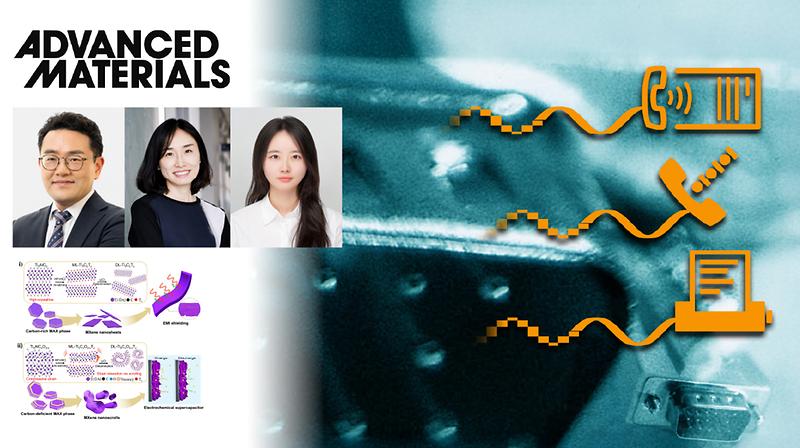
* 본 보도자료는 한국연구재단 주관으로 작성되었습니다. (바로 가기) □ 국내 연구진이 탄소 조성 제어로 꿈의 신소재 ‘맥신(MXene)*’을 정밀 제어해 초고주파 EMI(Electromagnetic Interference Shielding) 차폐**와 고속 에너지 저장 성능을 세계적 수준으로 끌어올려 주목을 받고 있다. * 맥신(MXene) : 금속과 탄소층이 교대로 쌓인 2차원 나노소재로, 전기전도성이 뛰어나고 다양한 화합물 설계가 가능해 배터리·반도체·센서 분야의 꿈의 신소재로 불림. ** 초고주파 EMI(Electromagnetic Interference Shielding) 차폐 : 차세대 6G 통신, 고해상도 차량용 레이다, 위성 통신 등에서 발생하는 고주파 영역의 전자파 간섭을 막아내는 핵심 기술. □ 한국연구재단(이사장 홍원화)은 울산과학기술원 권순용·최은미 교수 연구팀이 MAX 전구체*의 탄소 조성을 정밀 제어해 맥신의 구조와 기능을 합성 단계에서 선택적으로 설계하는 데 성공했다고 밝혔다. * MAX 전구체 : 맥신을 만들기 위한 전 단계의 초기 원료 물질(화합물) □ 이번 연구성과는 과학기술정보통신부와 한국연구재단이 추진하는 나노․소재기술개발사업의 지원으로 수행됐으며, 재료과학 분야 세계적 권위지인 ‘어드밴스드 머티리얼즈(Advanced Materials)’에 5월 18일 게재됐다. □ 6G 통신, 자율주행 레이더, 고집적 패키징 등 차세대 전자기기가 고주파 환경으로 빠르게 전환됨에 따라, 전자파 간섭으로 인한 오동작을 막아줄 초박막 차폐 기술의 필요성이 커지고 있다. ○ 그러나 기존 금속계 차폐재는 높은 차폐성에도 불구하고 무겁고 부식에 취약해, 유연·경량·초박막화를 동시에 요구하는 차세대 전자기기에는 제약이 있었다. 이러한 이유로 높은 전도도와 용액공정 적합성을 갖는 맥신 계열 소재가 대안으로 주목받고 있다. □ 최근 맥신의 전기적·구조적 특성을 근본적으로 제어하기 위한 전구체 수준의 조성·구조 설계가 핵심 기술로 주목받고 있다. 연구팀은 맥스 전구체의 탄소 조성을 정밀 제어하는 방법으로 맥신의 구조와 기능을 선택적으로 구현하는 데 성공했다. ○ 탄소가 풍부한 조건에서는 전기전도도가 우수한 평면 나노시트 구조가 형성되어, 100GHz 초고주파 대역에서 탁월한 전자파 차폐 성능과 뛰어난 굽힘 내구성을 나타냈다. ○ 반대로 탄소가 부족한 조건에서는 나노 스크롤 구조가 자발적으로 형성되어 이온 이동 통로가 확장되었으며, 이를 통해 고용량과 압도적인 수명 특성을 가진 고속 에너지 저장 성능을 확보했다. ○ 연구팀은 이번 연구 성과를 통해 전구체 조성 조절만으로 차폐용 평면 시트와 에너지 저장용 스크롤 구조를 하나의 플랫폼에서 맞춤형으로 설계할 수 있음을 입증했다. □ 박재은(제1저자) 연구원은 “평면 시트는 전자파 차폐에, 나노스크롤은 에너지 저장에 유리하다는 점을 실험적으로 입증해 하나의 소재 플랫폼에서 응용 방향을 나눠 설계할 수 있게 됐다”고 밝혔다. ○ 그리고 권순용 교수는 "지난해에는 질소 치환으로 맥신의 전도도와 광대역 차폐 성능을 끌어올렸다면, 이번에는 전구체 조성만으로 맥신 구조 자체를 설계하는 단계로 나아갔다”며, “초박막이면서도 100GHz 대역에서 높은 차폐 성능과 굽힘 내구성을 함께 보여, 차세대 6G·레이다 환경에 필요한 유연 차폐 소재 가능성을 확인했다”고 밝혔다.

원자력공학과, ‘원자력 안전규제라운드테이블’ 개최

연구 2026년 05월 14일 목요일

수개월 걸리던 반도체 설계, AI가 ‘단 하루’ 만에 끝낸다!

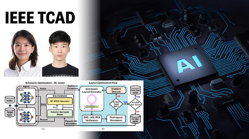
반도체 설계 전문가가 수주에서 수개월씩 걸려 작업하던 고성능 통신 반도체 회로 설계를 단 하루 만에 끝낼 수 있는 인공지능 기술이 개발됐다. UNIST 전기전자공학과 윤희인 교수와 경북대학교 송대건 교수팀은 통신 회로인 LC 전압제어 발진기(LC-VCO)를 회로 설계 단계부터 실제 칩에 넣는 물리적 레이아웃까지 자동으로 설계해주는 AI 모델을 개발했다고 5일 밝혔다. LC-VCO는 5G 같은 고속 통신 시스템에서 주파수를 만들어내는 반도체 회로다. 신호 잡음과 전력 소모를 줄이기 위해서는 인덕터, 트랜지스터 크기와 같은 변수를 잘 조합해 회로를 설계해야 하는데, 설계된 회로를 실제 칩 안으로 옮기기 위한 레이아웃 설계 단계에서는 회로 설계 단계의 조합이 깨지기 쉽다. 배선 굵기와 소자 배치에 따라 기생 효과가 더해지면서 주파수와 잡음 특성이 다시 달라질 수 있기 때문이다. 연구팀이 개발한 모델은 회로 설계와 레이아웃 설계를 통합해 최적화할 수 있다. 회로 설계 단계에서는 강화학습을 적용해 설계 변수들을 바꿔가며 목표 주파수와 성능을 만족하는 조합을 찾도록 했고, 실제 칩 구조가 결정되는 레이아웃 단계에서는 경사하강법을 이용해 배선 폭과 간격 같은 물리적 설계 변수를 성능이 개선되는 방향으로 반복적으로 보정하는 방식이다. 경사하강법은 현재 상태에서 성능이 더 좋아지는 방향을 따라 설계 값을 조금씩 조정해 최적의 조건을 찾아가는 최적화 기법이다. 연구팀은 “회로도 설계(Schematic)와 물리적 배치(Layout)를 개별적으로 최적화하던 기존 방식을 대신 AI가 두 단계를 통합적으로 관리하도록 한 기술”이라고 설명했다. 설계 과정에서 가장 시간이 오래 걸리는 인덕터는 딥러닝 기반 예측을 활용해 전체 설계 시간을 크게 줄였다. 설계자의 반복적인 전자기 시뮬레이션이 필요하던 작업을 단 몇 밀리초(ms) 만에 완료된다. 실험 결과, 기존의 자동 설계 방식이 약 119시간 소요되던 작업을 단 28.5시간 만에 완료해 설계 시간을 76% 이상 단축했다. 성능 지수(FoM) 또한 기존 연구 대비 월등히 우수한 결과를 보였다. 또 전이 학습이 적용돼 반도체 나노 공정 노드가 바뀌어도 기존에 학습한 내용을 바탕으로 설계를 이어갈 수 있다. 예를 들어 65nm 공정으로 학습한 AI는 40nm나 28nm 공정에서도 처음 학습에 필요했던 데이터의 약 10%만 추가로 활용해 설계를 수행할 수 있다. 공동 연구팀은 “5G·6G 통신과 AI 칩의 핵심 부품인 주파수 생성 회로의 성능은 높이면서 설계 비용은 크게 낮출 수 있을 뿐만 아니라 중장기적으로 반도체 설계 인력 부족 문제를 해결하고 차세대 공정으로의 전환 속도를 획기적으로 앞당길 수 있는 도구”라고 기대했다. 연구팀은 LC-VCO뿐만 아니라 다양한 아날로그/RF 회로 설계 자동화로 기술을 확장해 나갈 예정이다. 이번 연구는 UNIST 김성진 연구원과 경북대학교 이현수 연구원이 제1저자로 주도하였고 경북대학교 홍성민 연구원이 참여하였다. 연구 결과는 IEEE 반도체 회로 공학회에서 발행하는 권위 학술지인 ‘IEEE 집적회로 및 시스템 설계자동화(TCAD, Transactions on Computer-Aided Design of Integrated Circuits and Systems)’에 4월 3일 온라인 공개됐다. 연구는 과학기술정보통신부와 한국연구재단(NRF), 교육부(BK21 Four), 산업통상자원무(MOTIE), 반도체설계교욱센터(IDEC), 삼성전자, ㈜액시온 등의 지원 및 과기정통부와 정보통신기획평가원(IITP)의 '지역지능화혁신인재양성사업'의 지원으로 수행되었다.

원자력공학과, ‘원자력 안전규제라운드테이블’ 개최

대학소식 2026년 03월 13일 금요일

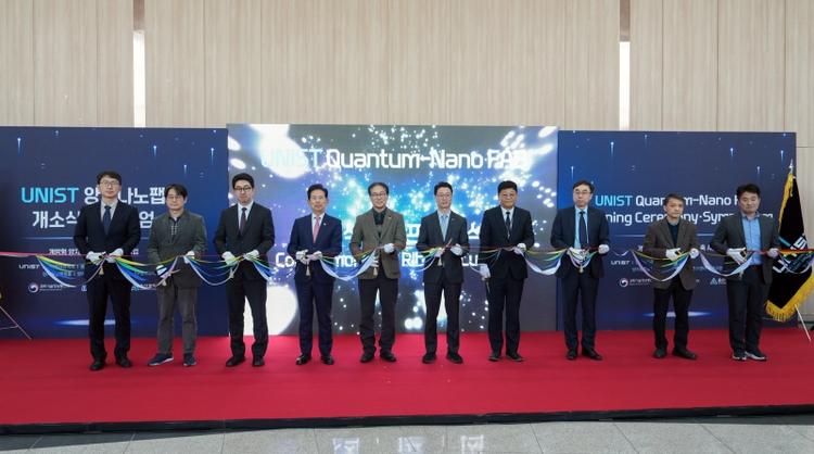
UNIST 양자나노팹 개소… "울산에 국가 양자 인프라"

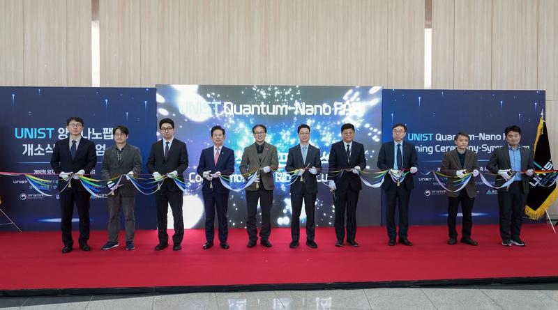
대한민국 양자기술 경쟁력 강화를 위한 국가 핵심 연구 인프라가 UNIST에 들어섰다. 13일, 총 300억 원 규모의 국가 양자 소자 개발 시설인 ‘UNIST 양자나노팹(Quantum-Nano FAB)’이 문을 열었다. 이날 108동 1층에서 열린 개소식·심포지엄에서는 양자 소자 설계부터 제작·분석·검증·실증까지 전 과정을 한곳에서 수행할 수 있는 원스톱 자율사용 연구 환경이 공개됐다. UNIST 양자나노팹은 과학기술정보통신부와 정보통신기획평가원(IITP)이 지원한 두 개 사업으로 조성됐다. 양자 소자 설계·제작·분석·검증·실증까지 이어지는 연구 전주기를 한 공간에서 수행할 수 있도록 공정 장비와 분석 체계를 통합한 것이 특징이다. 이 시설은 UNIST가 18년간 운영해 온 개방형 나노팹을 기반으로 구축됐다. UNIST 나노팹은 전국 60여 개 기관이 공동 활용하는 연구 공정을 연간 3만3000여 건 수행하고 매년 800여 명의 자율사용 연구자를 배출해 왔다. 여기에 양자 공정 특화 장비와 전담 지원 체계를 추가하면서 ‘UNIST 양자나노팹’으로 기능을 확장했다. 이번 양자나노팹 개소로 UNIST는 기존 나노 공정 중심 연구 환경에서 양자 소자 공정까지 아우르는 연구 거점으로 확대된다. 이를 바탕으로 울산을 양자·반도체 산업을 연결하는 동남권 혁신 허브로 육성한다는 계획이다. 산업 수도 울산은 자동차·조선·석유화학을 중심으로 발전해 왔지만 첨단 반도체 분야 기반은 상대적으로 부족했다. UNIST는 반도체대학원 설립과 나노팹 구축을 통해 산업 구조 전환의 토대를 마련해 왔으며, 이번 양자나노팹 개소를 계기로 울산을 미래 기술 표준을 창출하는 하이테크 연구·산업 도시로 발전시킨다는 구상이다. UNIST는 양자나노팹 운영 방향으로 △원스톱(One-Stop) △개방형(Openness) △비전(Vision) 등 세 가지를 제시했다. 설계부터 제작·분석까지 한 공간에서 수행하는 연구자 중심 환경이 원스톱 체계이며, 개방형은 60여 개 기관이 공동 활용하는 연구 협력 모델을 의미한다. 비전은 울산 산업 구조를 중화학 중심에서 양자·반도체 기반 첨단 산업으로 전환하는 미래 전략이다. 박종래 총장이 'UNIST 양자나노팹 개소식·심포지엄' 행사에서 환영사를 전하고 있다. 박종래 총장은 개소식 축사에서 “300억 원 규모 투자는 단순한 시설 확충이 아니라 대한민국 양자 기술 역량 강화를 위한 중요한 이정표”라며 “UNIST 양자나노팹을 울산에서 시작되는 양자 생태계의 핵심 플랫폼으로 성장시켜 연구 성과가 기술 고도화와 산업 성과로 이어지는 선순환 구조를 만들겠다”고 말했다. 정일석 교수(개방형 양자 인프라 구축사업 책임자)는 “UNIST 양자나노팹은 연구자들이 첨단 공정 장비와 분석 시설을 자유롭게 활용할 수 있는 중형 개방형 팹의 글로벌 모델이 될 것”이라며 “산·학·연 협력을 촉진하고 국내 양자 기술 연구의 공동 활용 거점으로 자리매김할 것”이라고 전했다. 이날 개소식에는 홍진배 정보통신기획평가원(IITP) 원장과 안효대 울산광역시 경제부시장 등 주요 내·외빈 80여 명이 참석했다. 행사에서는 양자 분야 전문가들이 최신 기술 동향을 공유하는 학술 심포지엄과 실제 공정 라인을 둘러보는 팹 투어(Fab Tour)도 함께 진행됐다.

원자력공학과, ‘원자력 안전규제라운드테이블’ 개최

연구 2026년 02월 24일 화요일

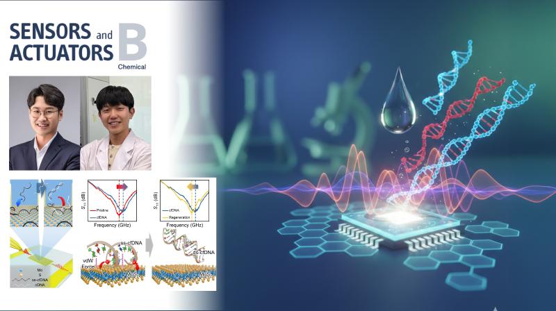
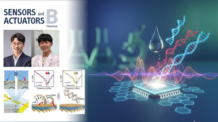
씻어서 또 쓸 수 있는 암 전이 잡아내는 센서 개발

씻어서 다시 쓸 수 있는 저렴한 센서를 이용한 액체 생검 기술이 개발됐다. 고가의 액체 생검 비용을 낮출 수 있게 됐다. UNIST 전기전자공학과 김명수 교수팀은 KAIST 신우정 교수팀, 연세대학교 강주훈 교수팀과 공동으로 이황화몰리브덴(MoS2)과 고주파(RF)를 이용해 재사용 가능한 고감도 액체 생검 센서를 개발했다고 12일 밝혔다. 액체 생검은 실제 조직을 떼어내지 않고도 혈액이나 체액 속에 떠다니는 DNA 조각을 감지해 암을 찾아내는 기술이다. 하지만 기존 검사법은 감지 센서가 일회용이거나 센서 제작 비용이 커 비용 부담이 있었다. 연구팀이 개발한 이황화몰리브덴 센서는 특수 용액에 씻어내기만 하면, 5회 재사용할 수 있다. 제작도 쉬워 공정 비용도 저렴하다. 이황화몰리브덴 잉크를 기판에 발라 회전시킨 뒤 잉크 속 용매를 날려버리기만 하면 된다. 진단은 센서에 환자 체액을 떨어뜨린 뒤 고주파(RF)를 쏘아 반응을 살피는 방식인데, 표적 DNA가 센서에 달라붙을 때 발생하는 유전율과 저항의 변화가 고주파 신호의 공진 주파수를 이동시키는 원리다. 개발된 센서는 기존 유전자 분석 기술이 놓치기 쉬웠던 '단일 가닥 DNA'만을 검출해낸다. 단일 가닥 DNA는 말기 암이나 림프절 전이 환자에게서 고농도로 발견되는 바이오마커다. 일반적으로 DNA는 단일 가닥이 서로 마주 보고 결합한 이중 나선 가닥 형태로 존재한다. 실험에서 이 센서는 암 진단 지표인 'AluSx1' 유전자 DNA 조각을 154.67nM (나노몰)의 매우 낮은 농도까지 정확하게 검출해냈다. [연구그림] 재사용 할 수 있는 액체 생검 센서의 구조와 작동 및 재생 과정 한편, 센서를 세척 하는 특수 용액에는 상보 염기가 들어가 있다. DNA의 이중 나선은 염기라는 분자가 서로 마주 보고 결합해 생긴 구조인데, 서로 짝을 이룰 수 있는 조합, 즉 상보 조합이 정해져 있다. 센서 표면에 붙어 있던 단일 가닥 DNA가 세척액 속의 짝을 만나 결합하면서 이중 나선이 완성되고, 이중 나선 DNA는 별도 처리 없이도 센서에서 저절로 떨어진다. 이번 연구는 김명수 교수와 신우정 교수가 교신저자로, UNIST 이승찬 연구원과 KAIST 최은호 연구원이 제1저자로 주도했다. 공동 연구팀은 “암 전이와 밀접한 단일 가닥 DNA를 저비용으로 검출할 수 있게 돼, 향후 실제 임상에서 암전이 조기 진단과 예후 모니터링 비용을 획기적으로 낮출 수 있을 것”이라며 “병원을 넘어 가정에서도 손쉽게 암 예후를 관리할 수 있는 자가 진단 기기와 스마트 헬스케어 시스템으로 발전시켜 나갈 계획”이라고 말했다. 이 연구성과는 한국연구재단 개인기초연구(신진연구) 국가아젠다 기초연구, 기초연구실지원사업, BRIDGE융합연구개발사업, 정보통신기획평가원(IITP)의 지역지능화혁신인재양성사업의 지원으로 수행되었으며, 센서 분야의 국제학술지인 ‘센서 앤 액추에이터 B: 케미컬(Sensors and Actuators B: Chemical)’에 1월 22일에 온라인 게재됐다.

원자력공학과, ‘원자력 안전규제라운드테이블’ 개최

연구 2026년 02월 24일 화요일

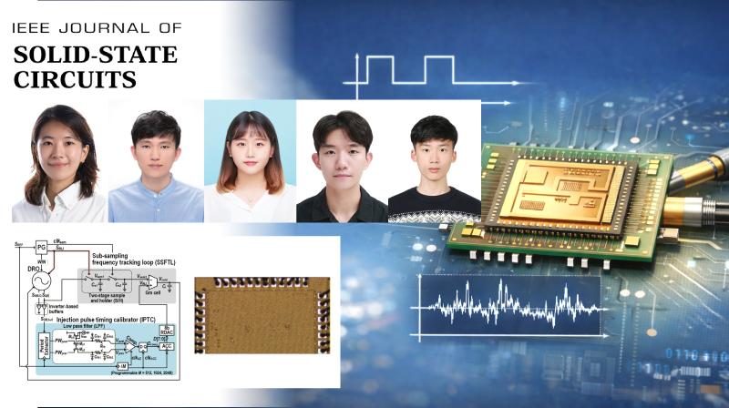
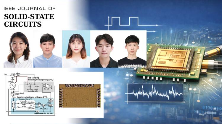
반도체 고속 작동 ‘칼박자’ 맞춰주는 클록 신호 생성 기술 개발

반도체 칩 안의 수십억 개의 소자들은 ‘클록’이라는 신호에 맞춰 일사불란하게 작동해야 한다. 데이터를 고밀도로 압축해 고속으로 주고받는 5G·6G 통신이나 고속 연산이 필요한 AI 칩의 경우 클록 신호의 품질이 더 중요해지는데, 고품질 클록 신호를 만들 수 있는 초소형·저전력 반도체 회로 기술이 새롭게 개발됐다. UNIST 전기전자공학과 윤희인 교수팀은 잡음을 획기적으로 줄인 ILCM (Injection-Locked Clock Multiplier) 기반 클록 신호 생성 반도체 회로를 개발했다고 11일 밝혔다. 반도체 칩은 ‘클록(Clock)’이라는 주기적 전기 신호에 맞춰 데이터를 처리한다. 특히 5G·6G 고속 통신칩이나 AI칩처럼 방대한 데이터를 빠르게 처리해야 하는 환경일수록 클록 신호의 품질은 시스템의 성능과 직결된다. 연구팀은 참조 스퍼(Reference spur)라는 잡음을 최소화할 수 있는 ILCM 방식의 클록 신호 생성 회로를 개발했다. ILCM 방식은 클록 신호의 지터(Jitter)라는 잡음은 최소화할 수 있지만 참조 스퍼라는 또 다른 잡음이 필연적으로 발생하는데, 이를 해결한 기술이다. 특히 ILCM 중에서도 소형화에 강점이 있는 링 발진기(Ring VCO) 기반 ILCM 방식을 채택해, 고집적 반도체 칩을 만드는 데 유리하다. 개발된 반도체 회로의 참조 스퍼는 2.1GHz 출력 조건에서 –81.36dBc(반송파 기준 데시벨)를 기록했다. 이는 현재까지 보고된 링 발진기 기반 ILCM 회로 중 세계 최저 수준이다. 지터 역시 280.9펨토초(fs, 1000조 분의 1초)를 달성해 초고속 작동에 적합함을 입증했다. 또 회로 면적도 28nm CMOS 공정으로 제작했을 때 0.0444mm²로 작고, 전력 소모 또한 12.28mW(밀리와트)로 최소화해 공간 제약이 크고 배터리 효율이 중요한 모바일 기기나 사물인터넷(IoT) 센서에 쓸 수 있다. [연구그림] 개발된 클록 생성 반도체 회로의 구조(상단)와 실제 사진 한편, 클록 신호는 저전압과 고전압이 심박처럼 반복되는 주기 형태로, 저전압과 고전압 반복 주기가 1초에 수억 번(MHz)에서 수십억 번(GHz) 수준으로 빠르다. 지터는 이 반복 주기가 일정하지 않은 일종의 ‘신호 주기 오차’다. 고속 통신 칩이나 AI 칩에서는 클록 신호 주기를 더 단축하고, 정확성을 유지하기 위해 깨끗한 참조 신호(Reference)를 강제로 주입해 오차를 보정 하는 방식을 쓰는데, 이 과정에서 신호가 주입될 때마다 ‘참조 스퍼’라는 잡음이 남게 된다. 연구팀은 주파수 추적(SSFTL)과 기준 신호 주입 타이밍 보정(IPTC) 설계방식을 적용해 이 같은 회로를 개발했다고 설명했다. 이번 연구는 남현준, 안효경 연구원이 제1저자로 참여했다. 연구팀은 “ILCM 방식의 클록 생성은 빠르고 효율적이지만 참조 스퍼가 시스템 성능을 제한하는 경우가 많았다”며 “이번에 개발된 기술은 단순한 회로 구조로 참조 스퍼는 최소화하면서도 전력 소모는 크지 않아 6G·AI·고속 인터커넥트용 클록 소스로 폭넓게 활용될 수 있을 것”이라고 말했다. 연구 결과는 IEEE 반도체 회로 공학회에서 발행하는 반도체 회로설계 분야 저명 학술지인 ‘저널 오브 솔리드 스테이트 서킷(Journal of Solid-State Circuits)’에 2월 6일 게재 됐다. 연구는 과학기술정보통신부, 반도체설계교육센터 (IDEC), 과학기술정보통신부와 정보통신기획평가원(IITP)의 '지역지능화혁신인재양성사업'의 지원으로 이뤄졌다.

원자력공학과, ‘원자력 안전규제라운드테이블’ 개최

연구 2026년 01월 20일 화요일

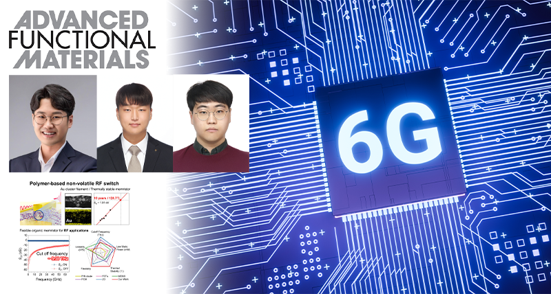
“비닐처럼 유연한데 열에도 강하다”... 고성능 6G 통신 소자 개발

비닐처럼 얇고 유연하면서도 뜨거운 열을 견딜 수 있는 차세대 고성능 통신 반도체 스위치가 개발됐다. 고온의 열기나 쉴 새 없이 구부러지는 충격 등 가혹한 환경을 버텨야 하는 웨어러블 기기, 자율주행차에서도 안정적인 5G·6G 통신을 가능하게 할 기술로 주목받고 있다. UNIST 전기전자공학과 김명수 교수팀은 단국대학교 김민주 교수팀과 공동으로 고성능 유연 RF 스위치를 개발했다고 8일 밝혔다. RF 스위치는 신호 간섭을 막고 전력을 효율적으로 배분하는 통신 부품이다. 상용화된 RF 스위치는 딱딱하고, 접히면 금 가기 쉬운 무기물을 기반으로 한다. RF 스위치를 기기의 접히지 않는 곳에 배치하는 방식으로 ‘폴더블 휴대폰’은 만들 수 있어도, 완전히 돌돌 말리거나 입을 수 있는 수준의 통신 기기를 만들 수 없었던 이유다. 연구팀이 개발한 RF 스위치는 비닐처럼 얇고 유연한 고분자를 기반으로 함에도 불구하고 내열성이 뛰어나고, 무기물 RF 스위치와 맞먹는 통신 성능을 지녔다. 일반적인 유기고분자 RF 소자는 유연한 장점이 있지만, 열에 잘 녹고 무기물 RF 소자보다 통신 성능이 떨어진다. 특히 5G·6G 대역에서 통신 성능 저하가 심하다. [연구그림] 고분자 기반 유연 RF 스위치의 구조와 내열 및 고주파 대역 성능 검증 결과 실제 실험에서 이 RF 스위치는 128.7℃의 고온 환경에서도 10년 이상 데이터가 유지될 수 있는 수준의 안정성을 보였다. 통신 성능 검증 실험에서는 5G와 6G 통신의 주요 주파수 대역인 밀리미터파(mmWave) 대역을 포함해 최대 5.38테라헤르츠(THz)까지 신호를 안정적으로 전달하고 차단할 수 있었다. ‘5.38테라헤르츠’는 고분자 기반 스위치가 처리할 수 있는 주파수 대역 중 가장 넓은 범위로, 현존하는 유기 고분자 스위치 중 최고 수준의 성능이다. 또 3,600회 이상 반복해서 굽혀도 성능 저하 없이 정상 작동해 탁월한 유연성을 증명했다. 연구팀은 특수 고분자 소재인 ‘pV3D3’를 이용해 이 같은 RF 스위치를 개발할 수 있었다. ‘pV3D3’ 라는 소재는 3차원 그물망 구조라 열에 강하다. 이 소재를 머리카락보다 가는 금박 사이에 적층시켜 RF 스위치를 만들었다. 전압이 가해지면 금박에서 빠져나온 이온이 이동하면서 전기가 흐르는 길이 만들어지고, 전압 방향이 바뀌면 이 통로가 끊어지면서 전류가 차단되는 방식으로 작동한다. 기계적 스위칭 없이 전류 흐름을 껐다가 켜는 멤리스터 방식이다. 이번 연구는 UNIST 박성문, 표창우 연구원과 단국대학교 유지호 연구원이 제1저자로 참여했다. 연구팀은 “기존 전자 소자가 가진 열적 불안정성과 고주파 성능 한계를 동시에 극복했다는 점에서 의미가 크다”고 설명했다. 김명수 교수는 “이번 연구는 유연 소자는 열에 약하고 성능이 떨어진다는 편견을 깬 사례”라며 “향후 고온이나 굴곡진 환경에서도 작동해야 하는 차세대 웨어러블 통신 기기나 IoT 센서, 자율주행차량의 통신 시스템에 폭넓게 적용될 수 있을 것”이라고 기대했다. 이 연구성과는 한국연구재단 개인기초연구(신진연구), 정보통신기획평가원(IITP)의 지역지능화혁신인재양성사업의 지원으로 수행되었으며, 재료 과학 분야의 세계적 권위지인 ‘어드밴스드 펑셔널 머티리얼즈(Advanced Functional Materials, IF: 19.0)’에 지난달 12일 게재됐다.

원자력공학과, ‘원자력 안전규제라운드테이블’ 개최

연구 2025년 12월 24일 수요일

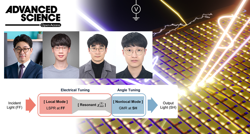
‘모래알’만한 칩으로 빛 파장, 밝기 마음대로 바꾼다!

빛의 파장과 세기(밝기)를 서로 간섭 없이 조절할 수 있는 모래알만 한 칩이 나왔다. 실시간으로 파장과 세기를 조절해야 하는 ‘양자 얽힘 광원’이나, 소형화가 필수적인 ‘광신호 처리 장치’ 등을 만들 수 있게 됐다. UNIST 전기전자공학과 이종원 교수 연구팀은 빛의 ‘세기’와 ‘파장’을 각각 독립적으로 제어할 수 있는 새로운 ‘메타표면’ 소자를 세계 최초로 개발했다고 16일 밝혔다. 메타표면(Metasurface)은 빛의 파장보다 훨씬 작은 나노 구조물을 표면에 배열해, 빛의 광학적 성질을 자연계에 없는 방식으로 조절하는 미세 인공 소자다. 상용 광변조 기술에 쓰는 부피가 큰 매질을 대체해 각종 기기를 경량화할 수 있고, 기존 광변조 기술로는 불가능한 광학 현상을 만들 수 있다 연구팀이 개발한 메타표면은 ‘제2고조파 생성(SHG)’이라는 특수한 광학 현상을 제어한다. 제2고조파 생성은 입력된 빛(기본 파장)의 에너지를 두 배로 증폭시켜, 파장이 절반인 새로운 빛(제2고조파)으로 변환해 출력하는 기술이다. 예를 들어 적외선 영역의 빛을 입력하면 파장이 다른 빛으로 변환되어 나오는데, 이는 미량의 생체 분자 감지하는 센서나, 도청이 불가능한 양자 통신 기술 개발에 쓸 수 있다. 하지만 지금까지 이 기술은 빛의 파장과 세기가 서로 복잡하게 얽혀 있다는 단점이 있었다. 변환 효율을 높여 빛의 세기를 강하게 만들려고 하면 파장을 조절할 수 있는 범위가 좁아지고, 반대로 파장 제어 범위를 넓히려면 효율이 급격히 떨어지는 상충 관계에 빠진 것이다. 연구팀은 메타표면 안에서 빛이 처리되는 과정을 ‘입구’와 ‘출구’로 분리하는 소자 설계 전략으로 이를 해결했다. 빛이 칩 안으로 들어와 에너지가 모이는 과정(생성)과 변신을 마치고 밖으로 나가는 과정(방출)을 서로 다른 제어 방식이 담당하도록 역할을 분담시킨 것이다. 연구팀은 이를 ‘로컬-투-논로컬(local-to-nonlocal)’ 방식이라고 명명했다 . 이렇게 설계된 메타표면 칩은 두 가지 독립된 제어 방식을 갖는다. 우선 칩에 흐르는 전압을 조절하면 빛의 파장은 변하지 않은 채 ‘세기’만 독립적으로 변하게 된다. 반대로 빛이 칩에 들어오는 각도를 살짝 비틀어주면 이번에는 세기는 그대로 유지되면서 빛의 ‘파장’만 변한다. 서로 간섭 없이 빛의 성질을 완벽하게 분리하여 조절하는 셈이다. [연구그림] 메타표면 소자가 빛의 색(파장)과 밝기(세기)를 조절하는 원리를 보여주는 개념도 실제 실험 결과, 연구팀이 빛의 입사각을 조절하자 출력되는 빛의 파장이 연속적으로 변했고, 특정 파장을 고정한 상태에서 전기 신호만 바꾸자 파장은 그대로 유지된 채 세기만 달라지는 것이 확인됐다. 이종원 교수는 “기존 연구들이 빛을 가두거나(로컬 모드) 흐르게 하는(논 로컬 모드) 한 가지 방식에만 의존했다면, 이번 기술은 두 방식을 결합해 소자 설계를 훨씬 자유롭게 만들고, 그동안 피하기 어려웠던 효율과 조절 능력 사이의 딜레마를 해결했다”고 설명했다. 이교수는 이어 “양자 정보를 실시간으로 제어하거나, 양자 통신의 핵심인 ‘얽힘 광자’의 파장 스펙트럼을 자유자재로 조절하는 등 차세대 능동형 양자 광원 기술을 완성하는 데 기여할 것”이라고 기대했다. 이번 연구는 어드밴스드 사이언스(Advanced Science)에 11월 29일 일자로 게재되었으며, 정보통신기획평가원과 한국연구재단의 지원을 받아 수행됐다.

원자력공학과, ‘원자력 안전규제라운드테이블’ 개최

대학소식 2025년 12월 16일 화요일

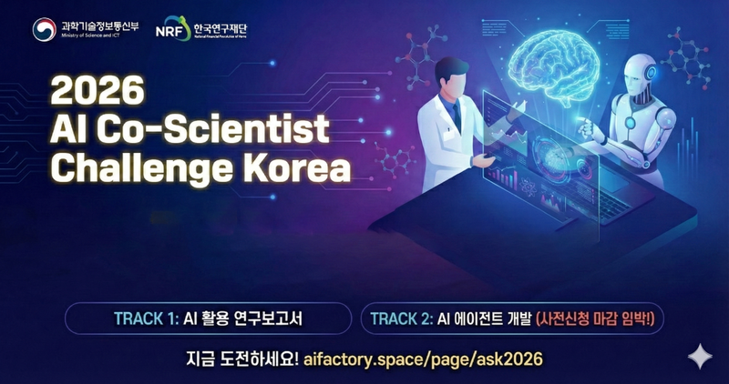
“챗GPT랑 함께한 연구결과물 제출하고 상금 받아가세요!”

과학기술정보통신부가 2026 AI Co-Scientist Challenge Korea 참가팀을 모집한다. 과학기술 연구에 AI를 효율적으로 활용할 수 있는 방법을 모색하고 더 나아가 연구동료로서 AI의 가능성과 한계를 탐색하기 위한 시도다. 이번 대회는 국내‧외 기업, 연구자, 학생 누구나 참여할 수 있으며, 상용 AI를 활용한 연구결과를 겨루는 Track 1, 직접 연구 도우미 AI 에이전트를 개발하는 Track2로 나눠 진행된다. Track1 참가자들은 상용 LLM이나 AI 에이전트를 활용해 바이오, 반도체 등 7대 분야의 지정주제 또는 자유 주제로 연구를 진행하고, 논문 형태의 연구보고서를 제출하면 된다. 이 때 AI 활용보고서(URL, 로그, 체크리스트 등 포함)와 활용 데이터 목록도 함께 제출해야 한다. Track1 부분은 총 6점의 수상작을 선발할 계획이며, 대상인 과학기술정보통신부장관상 수상자에는 500만원의 상금이 주어진다. Track2 부분의 사전 심사를 통과한 10개 팀에게 AI 모델 개발에 필요한 GPU, API 이용 비용 등을 제공한다. 총 10점의 수상작을 선발할 계획이다. Track2 대상팀은 500만원의 상금 뿐만 아니라 향후 연간 5억 원 규모의 ‘딥사이언스 창업 활성화 지원’(최대 3+2년, 기업) 또는 ‘공공연구성과 실증 시범사업’(2년, 연구자) 등 대형 후속 사업화 과제와 연계되는 특전이 주어진다. Track1은 이달 10일부터 내년 1월 31일까지, Track2의 사전 제안서는 내년 1월 2일까지 대회 공식 누리집(https://aifactory.space/page/ask2026)을 통해 온라인으로 접수하면 된다. 문의는 대회공식 누리집을 통해서 가능한다.

원자력공학과, ‘원자력 안전규제라운드테이블’ 개최

Research 2026년 07월 14일 화요일

New Wearable Patch Combines Multimodal Sensing with On-Chip AI

Abstract A proposed chest patch device and its interface IC are configured to allow detection of multi-domain signals in the form of optical, electrical, acoustic, and chemical signals at a single body spot. The IC integrates on-chip classification capabilities for cardiovascular diseases (CVDs) based on photo-plethysmogram (PPG) and electrocardiogram (ECG), along with hazardous gas analysis. For low-power multimodal sensing, an ECG R-peak_triggered PPG window (RPT-PW) is proposed as an inter-sensor scheme to reduce activity on the PPG channel, which is the dominant energy consumer. Additionally, the PPG and ECG readout channels incorporate analog peak detection to enable normalized on-chip extraction of pulse arrival time (PAT) and RR interval (RRI). For minimal computation and communication power, a multi-domain convolutional neural network (MD-CNN) processes both analog and digital inputs, and a reconfigurable analog ternary/binarized neural network (a-TNN/BNN) provides additional computation capability for multi-domain applications. The IC was fabricated in an 180-nm BCD process and integrated into a chest patch device prototype with an in-house adhesive meta patch. The RPT-PW demonstrated adaptive operation with an effective LED duty cycle (EDC) as low as 0.02%. The on-chip computation achieved average sensitivity and specificity of 90.87%/95.38% for three-label hypertension, 92.80%/96.36% for three-label arrhythmia, and 92.46%/97.50% for four-label gas mixture classification. Continuous wearable monitoring often requires transmitting large volumes of sensor data to external devices for analysis, increasing power consumption and limiting operating time. A joint research team, led by Professor Jae Joon Kim of Electrical Engineering and Professor Hoon Eui Jeong of Mechanical Engineering, has developed a wearable chest patch that analyzes physiological and environmental signals directly on the device, reducing both communication and sensing power while enabling continuous real-time monitoring. The wearable integrates optical, electrical, acoustic, and chemical sensing into a single device capable of simultaneously monitoring cardiovascular signals and hazardous gases. Rather than transmitting raw sensor data, it processes the information using an on-chip AI processor and sends only the analysis results via Bluetooth. This reduces communication overhead while allowing multiple users to be monitored remotely. To extend battery life, the researchers introduced an adaptive sensing scheme that selectively activates the optical sensor—the most power-intensive component of the device. By synchronizing optical measurements with ECG signals, the system reduced power consumption in the optical sensing channel by approximately 83%, enabling longer operation on a single charge. The device achieved more than 90% sensitivity and specificity in classifying hypertension and cardiac arrhythmias. It also classified hazardous gas mixtures with 92.46% accuracy, demonstrating its ability to monitor both physiological conditions and environmental hazards using a single wearable platform. The chest patch incorporates a microstructured adhesive interface that conforms securely to rough skin while allowing clean removal without leaving residue, making it better suited for long-term wear. “This work brings multimodal sensing and AI inference together on a single wearable platform,” said Professor Kim. “By processing information directly on the device, the system reduces communication demands while enabling continuous monitoring of both health conditions and environmental hazards.” The study has been participated by Sanghyeon Cho and Hyunjoong Kim as co-first authors. Their findings will appear in the July 2026 issue of the IEEE Journal of Solid-State Circuits (JSSC) , one of the leading journals in integrated circuit design. The technology has been licensed to Anvix Lab, a startup co-founded by the research team, which is pursuing commercialization of next-generation bioelectronic patch platform based on on-chip AI. The research was supported by the Ministry of Trade, Industry and Energy (MOTIE), the Ministry of Education (ME), and the Ministry of Science and ICT (MSIT). Journal Reference Sanghyeon Cho, Hyunjoong Kim, Dong Kwan Kang, et. al., “An Energy-Efficient Chest Patch Interface With Inter-Sensor PPG Windowing and Multi-Domain On-Chip Analog Computing,” JSSC , (2026).

원자력공학과, ‘원자력 안전규제라운드테이블’ 개최

Research 2026년 07월 02일 목요일

New Semiconductor Device Brings Communication and AI Computing onto a Single Chip

Abstract Next-generation 6G communication systems necessitate hardware that simultaneously manages high-frequency signal routing and massive matrix-level computations under extreme constraints. However, conventional digital architectures suffer from high power dissipation and area overhead. Here, we report an oxidized molybdenum disulfide (MoS2)-based memristive platform that integrates nonvolatile radio-frequency (RF) switching and energy-efficient vector–matrix multiplication. By implementing a controlled thermal oxidation process, we achieve stable resistive switching with low switching energy and zero-static power consumption, while maintaining a high cutoff frequency of 33.2 THz, outperforming existing phase-change and microelectromechanical systems (MEMS) technologies. Using system-level simulations, we demonstrate the robustness of this hardware through successful 1024-quadrature amplitude modulation (1024-QAM) demodulation, spectral analysis, and multiple-input multiple-output (MIMO) signal reconstruction, even when accounting for intrinsic device non-idealities. This monolithic integration of high-frequency switching and analog computing provides a scalable solution for energy-efficient deployment of intelligent wireless systems. Future 6G networks and satellite communication systems will require hardware that can process growing amounts of data while operating under strict power and space constraints. Professor Myungsoo Kim and his research team from the Department of Electrical Engineering at UNIST introduced a new semiconductor device that combines high-frequency signal switching and computation on a single platform, offering a more compact and energy-efficient approach to next-generation wireless systems. At the heart of the platform is a multifunctional memristor based on oxidized molybdenum disulfide (MoS2), a two-dimensional semiconductor. The device functions as both a radio-frequency (RF) switch and hardware for in-memory matrix operations, bringing communication and computation onto a single chip. Conventional communication systems typically separate these functions, requiring signals to move between switching circuits and processors. This data movement increases power consumption, processing delays, and chip size. By integrating both functions into a single device, the new platform simplifies signal processing while improving energy efficiency. The memristor also operates without standby power. Once switched between its ON and OFF states, it retains that state even after power is removed, making it particularly well suited to energy-constrained applications such as satellite communications and future 6G infrastructure. The device demonstrated a switching energy of just 140 picojoules per operation and switching power below one milliwatt. It maintained stable operation for more than 40,000 seconds and over 1,000 switching cycles, while achieving a calculated cutoff frequency of 33.2 THz. Experimental measurements verified high-frequency switching up to 67 GHz. To evaluate its computing capability, the researchers performed system-level simulations of wireless communication tasks. The device successfully carried out 1024-quadrature amplitude modulation (1024-QAM) demodulation and multiple-input multiple-output (MIMO) signal reconstruction, demonstrating that a single hardware platform can efficiently support both communication and signal processing. "Commercial RF switches continuously consume standby power and often suffer signal loss at high frequencies," said Juhyo Son, the study's first author. "Our device addresses these limitations while remaining competitive with existing phase-change memory and MEMS technologies in energy efficiency, operating speed, and scalability." Professor Kim added, "Our study demonstrates that oxidized MoS₂ memristors can function not only as high-performance RF switches but also as hardware for the in-memory matrix operations required for next-generation wireless communications. By combining nonvolatile operation, low power consumption, and high-frequency performance, this platform could contribute to more compact and energy-efficient systems for satellite communications, radar, defense electronics, and future 6G RF front ends." The research was supported by the National Research Foundation of Korea (NRF) through the Ministry of Science and ICT (MSIT), the Institute for Information & Communications Technology Planning & Evaluation (IITP), the Space-K BIG Project, and a regional talent development program. The findings were published online in Advanced Functional Materials on June 6, 2026. Journal Reference Juho Son, Changwoo Pyo, Sungmoon Park, et al., “ Oxidized MoS2-Based Multifunctional Memristive Hardware for Energy-Efficient mmWave Signal Processing and In-Memory Matrix Multiplication ,” Adv. Funct. Mater., (2026).

원자력공학과, ‘원자력 안전규제라운드테이블’ 개최

News 2026년 06월 09일 화요일

UNIST Selected to Lead National Space-K BIG Project for Very Low Earth Orbit Satellites

UNIST has been selected to lead a major national research project aimed at developing core technologies for very low Earth orbit (VLEO) satellite platforms, reinforcing Korea's efforts to strengthen its space technology capabilities. The project is part of the 2026 Space-K BIG Project, an initiative of the Korea AeroSpace Administration (KASA) that designs leading university research centers to advance foundational space technologies while training the next generation of space professionals. Under the program, the Department of Electrical Engineering at UNIST will receive KRW 5.7 billion in government funding through December 2030. The project, led by Professor Gangil Byun from the Department of Electrical Engineering , brings together Professors Myungsoo Kim, Hoon Lee, Jinseok Park, Minho Choi, Dongyun Kam, Kawon Han, and Jaeyong Jeong in a multidisciplinary effort. Titled "Mission-Oriented Convergent Platform Technologies for Very Low Earth Orbit Satellites and Global Talent Development," the project will develop key technologies for future satellite missions, including space-qualified RF devices, AI semiconductors, and optoelectronic components. Researchers will also advance domestically developed commercial off-the-shelf (COTS) technologies for satellite applications and establish an integrated VLEO satellite platform for future mission deployment. Education and workforce development form another major component of the initiative. UNIST will collaborate with industry, government research institutes, and international partners to provide students with hands-on research experience through joint projects and specialized training, creating an integrated environment that connects education with advanced space research. “This project provides an important opportunity for UNIST to lead research on core technologies for very low Earth orbit satellites while cultivating globally competitive talent in space engineering,” said Professor Gangil Byun, the project's principal investigator. “By combining the expertise of our faculty with the innovative capabilities of our industry partners, we aim to deliver technologies that will contribute to the future growth of Korea’s space industry.”

원자력공학과, ‘원자력 안전규제라운드테이블’ 개최

Community 2026년 06월 05일 금요일

Professor Sung Whan Yoon Receives MSIT Commendation for Digital Talent Development

Professor Sung Whan Yoon of the Graduate School of Artificial Intelligence (AIGS) and Department of Electrical Engineering at UNIST has been honored with a Ministerial Commendation from the Ministry of Science and ICT (MSIT) for his contributions to digital talent development. The award recognizes his efforts to advance reliable AI technologies, while connecting AI education with real-world manufacturing challenges. A major challenge in applying AI to factories is the gap between the lab and the field. Data collected from actual equipment often differs from the data used to train a model. Changes in materials, machine conditions, operating methods, or data quality can all weaken model performance. In manufacturing, those errors can lead directly to production losses or safety risks. Professor Yoon has worked to address that problem through robust AI algorithms. Robust AI refers to machine learning systems that continue to perform reliably even when conditions change. Rather than pursuing high accuracy only under fixed conditions, his work focuses on AI that can make dependable decisions in real industrial environments. His research has also drawn international recognition. At the International Conference on Learning Representations (ICLR) 2025, one of the world’s leading AI conferences, his work on improving the stability of reinforcement learning models was selected for an oral presentation. Oral presentations at ICLR are typically reserved for roughly the top 2 percent of submitted papers. Reinforcement learning allows AI systems to improve decisions through trial and error. In manufacturing, it can help optimize equipment settings and production processes. But factories leave little room for unstable decisions, since one wrong choice can create cost and safety risks. Professor Yoon’s research showed how reinforcement learning models can become more stable under uncertain or changing field conditions, moving the technology closer to industrial use. Beyond research, Professor Yoon has also brought those advances into AI education for manufacturing professionals. Since joining UNIST, Professor Yoon has helped design and run AI programs for industry workers in Ulsan and the southeastern region. The programs are built around problems participants face in their own factories, turning actual production issues into hands-on AI projects. His team has applied reinforcement learning-based optimization methods to manufacturing and processing facilities. The work aims to improve equipment operations while maintaining process stability and safety. This link between AI training and workplace change was a key reason for the commendation. Professor Yoon currently serves as a project leader in the national AI Star Fellowship program. In partnership with SK Energy, he is developing core technologies for robust manufacturing AI that can be used in complex process industries, including petrochemicals. “High performance alone is not enough for AI to succeed in industry,” Professor Yoon said. “AI systems must remain stable even when conditions change. We will continue developing robust AI technologies and connecting them to manufacturing solutions and digital talent development.”

원자력공학과, ‘원자력 안전규제라운드테이블’ 개최

Research 2026년 06월 05일 금요일

New High-Efficiency Wireless Charging for Implantable Medical Devices

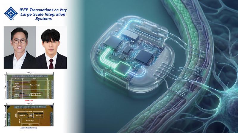
Abstract This article presents a single-input–dual-output (SIDO) wireless power transfer (WPT) system that maintains high link efficiency across both heavy and light load conditions. Conventional SIDO architectures employ a fixed matching network, which leads to significant efficiency degradation when the load changes. To address this limitation, the proposed system classifies the two outputs into heavy-load and light-load domains and employs dedicated matching networks optimized for each operating condition, thereby maximizing link efficiency during charging of either load. To minimize the power overhead of mode switching while enabling single-stage AC–DC regulation, a charging-phase controller, a full/half-window mode controller, and an adaptive window generator are employed. Furthermore, an active rectifier with a slowdown unit cell (SUC)-based on/off controller (SOOC) is proposed to improve power conversion efficiency (PCE). In addition, an early turn-on switching (ETS) is implemented to achieve higher PCE compared to conventional zero-voltage switching (ZVS). Fabricated in a 0.18- μ m BCD process, the system is implemented as two chips, a standalone rectifier for accurate PCE measurement and a SIDO integrating the same rectifier. The SIDO demonstrates stable full/half-window operation without multiple pulsing. Measured link efficiency reaches 94.4% at 3mA and 92.7% at 30mA at a coupling coefficient k = 0.2, confirming the effectiveness of the load-optimized matching. The rectifier achieves 94.5% peak PCE and maintains above 92.3% PCE across a 2.5–5.0V input range. A new wireless charging technology promises to enhance the safety and longevity of implantable medical devices, such as pacemakers and neural stimulators. Led by Professor Franklin Bien of the Department of Electrical Engineering, the research team developed a system that employs load-specific matching networks and adaptive control to optimize power delivery. Implantable devices often incorporate circuits with varying power demands—high-current circuits for stimulation and low-current circuits for data processing. Traditional wireless chargers rely on fixed configurations, which can lead to inefficiencies and heat buildup, potentially damaging surrounding tissue. The new system detects changes in load and switches between dedicated matching networks tailored for high and low power conditions, thereby optimizing energy transfer. Furthermore, the team improved the efficiency of the rectifier circuit that converts received alternating current (AC) into direct current (DC). By precisely controlling switching points during power conversion, they minimized energy loss and enhanced overall performance. Experimental results demonstrated a link efficiency of 94.4% at a low load of 3mA and 92.7% at a high load of 30mA. The active rectifier achieved a peak power conversion efficiency of up to 94.5%, maintaining above 92% even as input voltage varied from 2.5V to 5V. The research team anticipates that this technology will extend the operational lifespan of implantable devices, reducing the need for frequent surgical replacements and associated risks. It also holds promise for application in wearable electronics and compact Internet of Things (IoT) devices that require reliable, low-loss wireless power. The findings of this research were published online in the IEEE Transactions on Very Large Scale Integration (VLSI) Systems on April 29, 2026. The study has been s upported by the Ministry of Science and ICT (MSIT) and the Institute for Information & Communications Technology Planning & Evaluation (IITP). Journal Reference Sungmin Shin, Seongbin Kwon, Geonwoo Baek, et al ., “A Single-Input Dual-Output Wireless Power Transfer System With Load-Optimized Matching Network,” IEEE TVLSI. , (2026).

원자력공학과, ‘원자력 안전규제라운드테이블’ 개최

Research 2026년 06월 01일 월요일

Breakthrough Chameleon MXene Promises Advanced 6G Communication and Next-Gen Batteries

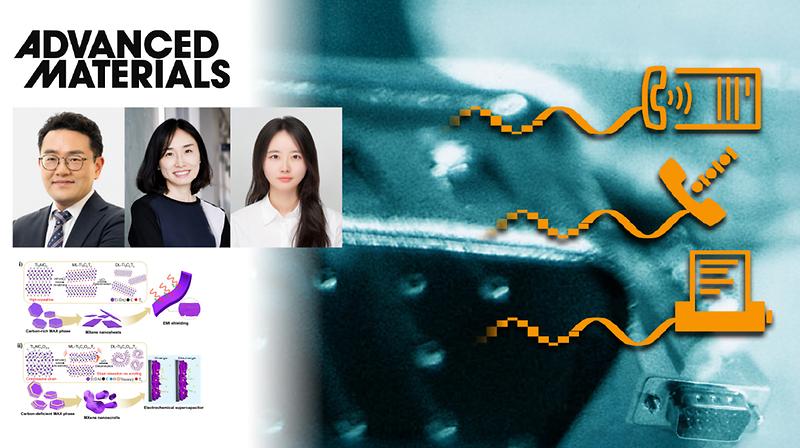
Abstract Device-level performance in MXenes is dictated by architecture—planar nanosheets are optimal for electromagnetic interference (EMI) shielding, while scrolled structures enhance ion transport for energy storage—particularly when morphology is programmed at synthesis. Whether such architectures can be deterministically encoded through precursor stoichiometry remains unresolved. Here, we demonstrate that precise carbon stoichiometry control in Ti3AlCxO2-x MAX phases tunes internal lattice strain and thereby directs the emergent MXene architecture. Carbon-rich precursors (x = 1.94) yield strain-relieved, high-crystalline nanosheets with metallic conductivity (∼23 300 S cm−1), enabling ultrathin films with record-high EMI shielding performances across 8 µm) and robust W-band retention after 5,000 bending cycles (r = 2.5 mm). In contrast, carbon-deficient precursors (x = 1.71) introduce lattice compression and oxygen substitution, triggering spontaneous scrolling upon delamination. The resulting nanoscrolls offer exceptional ion accessibility, achieving 657 F g−1 at 2 mV s−1 with 99.4% retention over 12 000 cycles. This stoichiometry-programmed approach establishes a synthesis-stage lever linking MAX chemistry to MXene architecture and function, enabling application-specific architecture design within established MAX/MXene synthesis and solution-processing workflows for next-generation electronics and energy storage. Researchers at UNIST have discovered a simple way to control MXene's structure by adjusting the carbon content in its precursor. This breakthrough enables the creation of tailored MXene materials optimized for high-frequency electromagnetic interference (EMI) shielding and rapid energy storage. MXene, a two-dimensional material composed of metal and carbon layers, is celebrated for its excellent electrical conductivity and adaptability. Its potential spans batteries, sensors, and flexible electronics. With the rise of 6G technology and advanced radar systems, shielding devices against high-frequency interference has become critical. At the same time, the demand for quick, reliable energy storage continues to grow. Led by Professor Soon-Yong Kwon from the Graduate School of Semiconductor Materials and Devices Engineering and Professor EunMi Choi from the Department of Electrical Engineering, the team showed that changing the carbon content in MAX precursors influences how MXene forms during synthesis. This control method results in two distinctly different structures. When using carbon-rich precursors, the process yields flat, highly crystalline nanosheets that exhibit excellent electrical conductivity, effective electromagnetic shielding at 100 GHz, and maintain flexibility and durability under repeated bending. Conversely, employing carbon-deficient precursors induces the spontaneous formation of nanoscrolls, which significantly enhance ion transport. These nanoscroll structures enable high-capacity energy storage, achieving a capacitance of 657 F/g and a cycle life exceeding 12,000 cycles. This work confirms that simple adjustments to precursor composition can produce MXene structures tailored for specific applications—flat sheets for shielding and scrolls for energy storage—within a streamlined process. First author Jaeeun Park explains, “We showed that flat MXene sheets are ideal for electromagnetic shielding, while scroll structures are better suited for energy storage. By controlling the precursor, we can design the material for different functions without changing the synthesis method.” Professor Kwon adds, "Last year, we enhanced MXene's conductivity and broadband shielding through nitrogen doping. Now, we've demonstrated how to design the material's shape from the start. The ultra-thin, flexible MXene performs well at 100 GHz and withstands bending, making it a promising lightweight, flexible shield for future 6G and radar systems." Supported by the Ministry of Science and ICT (MSIT) and the National Research Foundation of Korea (NRF), the study was published in Advanced Materials on May 18, 2026. Journal Reference Jaeeun Park, Ju-Hyoung Han, Yujin Chae, et al ., “Stoichiometry-Programmed MXenes via Precursor Engineering for High-Performance EMI Shielding and Energy Storage,” Adv. Mater ., (2026).

원자력공학과, ‘원자력 안전규제라운드테이블’ 개최

Research 2026년 05월 12일 화요일

Revolutionizing Semiconductor Design: AI Cuts Development Time from Months to Just One Day

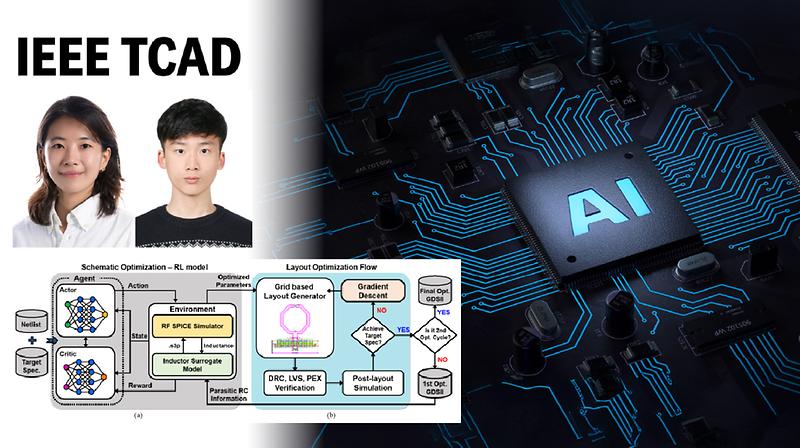
Abstract Artificial Intelligence (AI) has been increasingly utilized across various fields, including communications, healthcare, and Computer-Aided Design (CAD). However, AI has shown relatively limited advances in analog and RF circuit design, which are critical for modern communication systems such as 5G due to their higher complexity and nonlinear characteristics. For example, the Inductor-Capacitor Voltage-Controlled Oscillator (LC-VCO) is a crucial component in frequency synthesizers, determining the performance of RF systems, including high data transmission rates and wide bandwidth. In fact, LC-VCO design is challenging due to the high parameter variability and complex interactions between design variables, making it challenging to optimize parameters to meet target specifications. Thus, this study proposes a comprehensive LC-VCO design methodology compatible across multiple process nodes and supports optimization down to the layout level. We use Reinforcement Learning (RL) to navigate the nonlinear design space efficiently for schematic optimization and apply an algorithm from Gradient Descent to optimize the design at the physical layout level. We highlight that the versatility of our methodology is demonstrated by producing optimized Figures of Merit (FoM) across various technology nodes and frequency ranges, showcasing its potential as a universal design tool accessible to all users. A team of researchers from UNIST and Kyungpook National University (KNU) has unveiled a pioneering AI system capable of completing the complex design of high-performance semiconductor circuits in just one day—an achievement that drastically reduces the traditional development timeline, which can take several months. Led by Professor Heein Yoon of UNIST’s Department of Electrical Engineering and Professor Taigon Song of KNU, the team developed an integrated AI platform that automates the entire process—from schematic design to physical chip layout. This breakthrough technology streamlines a typically multi-stage, resource-intensive task, offering faster, more efficient, and highly optimized circuit design solutions. The initial focus was on the design of the Inductor-Capacitor Voltage-Controlled Oscillator (LC-VCO), a critical component in 5G and emerging 6G communication systems. LC-VCOs generate the carrier signals essential for high-speed data transmission. Designing these circuits involves balancing numerous variables—such as inductor and transistor sizes—to minimize noise and power consumption. However, translating schematic designs into physical layouts often introduces parasitic effects that can impair performance. The new model integrates circuit schematic optimization with physical layout design, addressing these challenges holistically. During the schematic phase, reinforcement learning algorithms explore various parameter configurations to meet specific frequency and performance targets. Subsequently, in the layout phase, the system employs gradient descent methods to iteratively refine physical design parameters—such as wire widths and spacing—to enhance overall circuit performance. Gradient descent, a well-established optimization technique, incrementally adjusts design variables by following the gradient of the objective function toward an optimal solution. This integrated approach drastically accelerates the design process. Tasks that previously required up to 119 hours can now be completed in approximately 28.5 hours—reducing the overall time by over 76%. Moreover, the system’s adaptability across different semiconductor process nodes is enabled by transfer learning. Models trained on one technology node (e.g., 65nm) can be efficiently adapted to others (such as 40nm or 28nm), using just around 10% additional data. This AI-driven methodology not only shortens development cycles and reduces costs but also addresses the industry’s growing need for efficient design automation amid a global talent shortage. By ensuring high performance while minimizing manual effort, this technology is poised to significantly impact the production of next-generation communication and AI chips. The researchers anticipate expanding this framework beyond LC-VCOs to automate various analog and RF circuit designs, further accelerating innovation in semiconductor technology. The research was led by Sungjin Kim of UNIST and Hyunsoo Lee of KNU, who served as co-first authors, with additional contributions from Hong Seong-min of KNU. The findings of this research have been published online in the IEEE Transactions on Computer-Aided Design of Integrated Circuits and Systems (TCAD) on April 3, 2026. The study has been supported by the Ministry of Science and ICT (MSIT), the National Research Foundation of Korea (NRF), the Ministry of Education (BK21 Four), the Ministry of Trade, Industry and Energy (MOTIE), the Semiconductor Design Education Center (IDEC), Samsung Electronics, Axion Co., Ltd., and the Institute for Information & Communications Technology Planning & Evaluation (IITP). Journal Reference Sungjin Kim, Hyunsoo Lee, Seongmin Hong, et al., "A Framework of Automated LC-VCO Design with Physical Layout Based on Reinforcement Learning, IEEE TCAD, (2026).

원자력공학과, ‘원자력 안전규제라운드테이블’ 개최

News 2026년 04월 13일 월요일

UNIST Launches Major AI Initiative to Transform Shipbuilding Industry

UNIST has launched a major interdisciplinary research initiative to accelerate AI-driven transformation (AX) across the shipbuilding sector. Selected under the Ministry of Science and ICT’s national initiative for large-scale industrial AI, the project is supported by a total budget of KRW 40.3 billion (approximately USD 30 million). It aims to develop domain-specific AI foundation models trained on real-world shipyard data and deploy them in operational environments. The initiative brings together faculty from the Graduate School of Artificial Intelligence (AIGS), along with multiple engineering and business disciplines, forming a collaborative structure that spans the full lifecycle of industrial AI—from data generation and model training to system deployment and real-world validation. At the core of the project is the development of a multimodal, domain-specific foundation model for shipbuilding. This effort is led by Professor Sung Youb Kim from the Graduate School of Semiconductor Materials and Devices Engineering, with participation from Professors Seung-Hoon Na, Youngsoo Jang, Seungryul Baek, and Taehwan Kim from AIGS, along with Professor Hayoung Chung from the Department of Mechanical Engineering. The team will develop a model capable of integrating diverse data generated across shipyard operations, serving as a central engine for a wide range of downstream applications. Complementing this effort, a parallel workstream led by Professors Sung Whan Yoon, Jae-Young Sim, and Yeon-Chang Lee from AIGS, along with Professor Saerom Park (Department of Industrial Engineering) and Professor Seongil Wi (Department of Computer Science and Engineering) will establish a scalable industrial platforms for optimized for heterogeneous datasets. In parallel, Professors Seungjoon Yang, Gi-soo Kim, and Yeon-Chang Lee from AIGS will lead research on synthetic data generation, addressing limitations in real-world data and improving model robustness across diverse scenarios. Application-focused research will be led by Professors Youngdae Kim, Sungil Kim, Hyungho Na, Dong Young Lim, and Chiehyeon Lim from the Department of Industrial Engineering, along with Professor Junghoon Kim (Department of Computer Science and Engineering), Professor Jinyoung Choi (AIGS), and Professor Junhyoung Ha (Department of Mechanical Engineering). Their work will focus on manufacturing optimization, production scheduling, predictive maintenance, and the intelligent operation of collaborative robotic systems. The development of lightweight, on-device AI technologies will be led by Professors Taesik Gong (Department of Computer Science and Engineering), Jongeun Lee (Department of Electrical Engineering), and Ranggi Hwang (Department of Computer Science and Engineering). Meanwhile, Professors Byeong Ki Seo (School of Business Administration) and Namhun Kim (Department of Mechanical Engineering) will oversee field validation and service deployment to ensure practical application and scalability. To ensure real-world impact, the initiative will be carried out in close collaboration with industry partners, including HD Hyundai Heavy Industries, HD Korea Shipbuilding & Offshore Engineering, and CrowdWorks. By leveraging operational data from active shipyards, the consortium will validate and refine technologies through on-site implementation. Professor Seung-Hoon Na, who coordinates the overall project, stated, “This initiative goes beyond developing AI models—it establishes a foundation for industrial AX. By integrating AI into production planning, process optimization, and quality control, we expect to drive meaningful innovation across the shipbuilding industry.” The UNIST Office of Research Affairs supported the initiative through its Pre-Award pilot program, providing strategic and administrative assistance in proposal development, budgeting, and coordination. The university plans to further advance its research management framework to support large-scale, high-impact initiatives.

원자력공학과, ‘원자력 안전규제라운드테이블’ 개최

Community 2026년 03월 27일 금요일

UNIST Secured Second Place at IEEE SaTML 2026

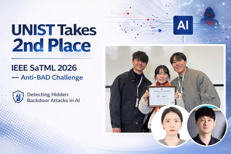
Researchers at UNIST has earned international recognition for developing a method to detect and mitigate hidden malicious triggers in artificial intelligence systems—an emerging threat to the reliability of large language models (LLMs). Led by Professor Saerom Park of the Department of Industrial Engineering and the Graduate School of Artificial Intelligence, and Professor Sung Whan Yoon of the Graduate School of Artificial Intelligence and the Department of Electrical Engineering, the team placed second in the Anti-Backdoor (Anti-BAD) Challenge at the IEEE Conference on Secure and Trustworthy Machine Learning (SaTML 2026), held in Munich, Germany, from March 23 to 25, 2026. Backdoor attacks embed hidden signals into AI models during training, causing them to produce unintended outputs when specific inputs—known as triggers—are encountered. Because these models otherwise perform as expected, these vulnerabilities present a persistent challenge for the safe deployment of AI systems. The competition challenged participants to develop methods, capable of reducing the impact of such triggers across a range of applications, including text generation, classification, and multilingual tasks. In response, the UNIST team proposed a unified framework designed to operate effectively across these varied settings. Their approach integrates model quantization, model merging, outlier parameter detection, and confidence calibration. Together, these techniques enable the identification and suppression of anomalous behaviors while preserving overall model performance. The methods does not rely on prior knowledge of attack patterns, making it applicable to a broad class of models and use cases. Contributors to the study include JiEun Yun and KiWan Kwon of the Department of Industrial Engineering, and SeungBum Ha of the Graduate School of Artificial Intelligence. "Even in the absence of prior information about the attack methods, it is possible to meaningfully reduce backdoor risks in large language models,” said JiEun Yun. "This work is a step toward ensuring that AI systems can be deployed with greater confidence." The IEEE SaTML is a leading international forum dedicated to advancing research on the security, robustness, and trustworthiness of machine learning systems. The annual competition serves as a benchmark for emerging approaches to safeguarding next-generation AI technologies.

원자력공학과, ‘원자력 안전규제라운드테이블’ 개최

News 2026년 03월 13일 금요일

New Quantum-Nano FAB at UNIST to Anchor Korea’s Open Quantum Research Ecosystem

UNIST has officially opened the UNIST Quantum-Nano FAB, a national research facility designed to accelerate quantum device development and strengthen South Korea's competitiveness in quantum technologies. The new infrastructure provides an integrated environment where researchers can design, fabricate, analyze, and validate quantum devices within a single facility, enabling the full lifecycle of quantum device research—from initial concept to experimental demonstration. Supported by the Ministry of Science and ICT (MSIT) and the Institute of Information & Communications Technology Planning & Evaluation (IITP), the facility represents a KRW 30 billion national investment in next-generation quantum research infrastructure. Furthermore, the facility integrates advanced nanofabrication equipment and analytical systems specifically optimized for quantum materials and devices. By bringing these capabilities together in one place, UNIST aims to provide researchers with a streamlined end-to-end research environment that supports rapid experimentation and collaboration. Approximately 80 distinguished guests attended the event, including President Jinbae Hong of IITP and Vice Mayor Hyo-Dae Ahn for Economic Affairs of Ulsan Metropolitan City. The UNIST Quantum-Nano FAB expands upon the university's long-standing open-access nano-fab infrastructure, which has been operated for more than 18 years. The existing platform supports collaborative research for over 60 universities, research institutes, and companies across Korea, handling approximately 33,000 fabrication processes each year and serving approximately 800 trained users annually. Supported by world-class analytical facilities and a team of more than 30 technical specialists, the platform has become a key hub for shared semiconductor and nanotechnology research in Korea. The addition of process equipment optimized for quantum device fabrication and dedicated support systems now extends these capabilities into the rapidly emerging field of quantum devices. President Jinbae Hong of IITP delivered a congratulatory remark at the opening ceremony of UNIST Quantum-Nano FAB on March 13, 2026. The launch of this facility also aligns with a broader regional vision to expand Ulsan's role in advanced technology industries. Known historically for its leadership in automotive, shipbuilding, and petrochemical manufacturing, Ulsan has been working to diversify into future technology sectors. Through initiatives such as the establishment of a Graduate School of Semiconductors Materials and Devices Engineering and the expansion of nanofabrication infrastructure, UNIST is helping position the region as a next-generation innovation hub linking quantum technology and semiconductor industries. UNIST outlined three guiding principles for operating the new facility: △ One-Stop—enabling researchers to carry out design, fabrication, and analysis within a single integrated facility. △ Open Access—providing shared research infrastructure available to universities, research institutes, and industry partners nationwide. △ Vision—supporting the long-term transition of Ulsan's industrial base toward advanced technologies, such as quantum computing and semiconductors. President Chong Rae Park described the initiative as an important milestone for the nation’s quantum research ecosystem. "This KRW 30 billion investment represents more than the construction of a new facility—it marks a significant step toward strengthening Korea’s capabilities in quantum technologies," said President Park. "We aim to develop the UNIST Quantum-Nano FAB into a core platform for a growing quantum ecosystem beginning here in Ulsan, where research breakthroughs can translate into technological advancement and industrial innovation." President Chong Rae Park delivered a welcome remark at the opening ceremony of UNIST Quantum-Nano FAB on March 13, 2026. Professor Il-Sug Chung (Department of Physics, UNIST), who led the open-access quantum infra development initiative, emphasized the importance of open-access and collaboration. "The UNIST Quantum Nano-Fab is designed as an open-access facility where researchers can freely utilize advanced fabrication and analysis equipment," said Professor Chung. "We expect it to serve as a collaborative hub connecting academia, industry, and research institutes while advancing quantum device development in Korea." The opening ceremony was accompanied by the UNIST Quantum-Nano FAB Inaugural Symposium, where leading researchers discussed emerging directions in quantum technologies. Speakers included Dr. Young Ho Lee, Director of the Center for Supercomputing Quantum Computing System at the Korea Research Institute of Standards and Science (KRISS) and Professor Jehyung Kim from the Department of Physics at UNIST. Approximately 80 distinguished guests attended the event, including President Jinbae Hong of IITP and Vice Mayor Hyo-Dae Ahn for Economic Affairs of Ulsan Metropolitan City. Participants also toured the fabrication facility, gaining a firsthand look at the equipment and research environment that will support next-generation quantum device development. The UNIST Quantum-Nano FAB Inaugural Symposium took place on March 13, 2026.

원자력공학과, ‘원자력 안전규제라운드테이블’ 개최

Research 2026년 02월 26일 목요일

Revolutionary Reusable MoS₂ RF Biosensor Enables Cost-Effective Liquid Biopsies for Early Cancer Detection

Abstract Reliable and cost-effective detection of single-stranded circulating cell-free DNA (ss-cfDNA) is crucial for liquid biopsies, offering a non-invasive method for precise cancer diagnosis and therapeutic monitoring. This work reports a reusable, label-free radio frequency (RF) biosensor utilizing solution-processed molybdenum disulfide (MoS2) thin films on an interdigitated capacitor. The spin-coating fabrication of the MoS2 layer offers superior scalability and cost-effectiveness compared to traditional 2D material growth and transfer. The sensing mechanism is initiated by the adsorption of ss-cfDNA nucleobases onto the MoS2 basal plane via van der Waals forces. This interaction concurrently induces n-type doping and alters the local dielectric environment, causing detectable impedance alterations manifested as resonant frequency shifts and time-domain reflection changes. The sensor achieves a limit of detection of 154.67 nM for a 20-base ss-cfDNA sequence from AluSx1, a key ALU element in cancer diagnostics, demonstrating high specificity for ssDNA over double-stranded DNA. Detecting ss-cfDNA of various lengths further validates the mechanism and establishes broad applicability. Moreover, the sensor demonstrates robust reusability (≥ 5 cycles) and 7-day stability using a complementary DNA-mediated regeneration process, which is comprehensively validated by a suite of analytical techniques. This solution-processable, label-free RF biosensor is a promising platform for cost-effective and scalable ss-cfDNA detection, distinguished by its simple fabrication, specificity, and reusability. A research team, affiliated with UNIST has unveiled an innovative, cost-effective biosensor capable of being washed and reused, paving the way for more accessible liquid biopsy diagnostics. This new platform aims to reduce the high costs and complexity associated with traditional cancer detection methods. Professor Myungsoo Kim from the Department of Electrical Engineering at UNIST, in collaboration with Professor Woojung Shin of KAIST and Professor Joohoon Kang of Yonsei University, announced the successful creation of a highly sensitive, reusable liquid biopsy sensor that leverages molybdenum disulfide (MoS₂) and radio frequency (RF) technology. Liquid biopsy is a non-invasive method that detects circulating tumor DNA fragments in blood or bodily fluids, enabling early cancer detection without the need for tissue removal. However, existing sensors are often single-use or expensive to produce, limiting their widespread clinical application. The new MoS₂-based sensor addresses these challenges by offering easy regeneration and low manufacturing costs. Its fabrication involves applying MoS₂ ink onto a substrate and then removing the solvent—an approach that is simple, scalable, and cost-effective. Figure. Schematic illustration of the MoS2-based RF sensor. During testing, the sensor analyzes a patient's bodily fluid using RF signals to monitor changes in electrical properties. When target DNA binds to the sensor surface, it causes shifts in permittivity and resistance, which alter the resonant frequency of the RF signal—enabling precise and label-free detection. Remarkably, the sensor can selectively detect single-stranded DNA (ssDNA), a vital biomarker for advanced-stage cancers and lymph node metastasis that are often missed by conventional methods. In experiments, it accurately detected the cancer-related AluSx1 DNA fragment at concentrations as low as 154.67 nanomolar. The detection mechanism relies on the base pairing of DNA. The sensor can be washed with a solution containing complementary DNA bases, which re-form the double helix and naturally detach the ssDNA, allowing the sensor to be reused up to five times without significant performance loss. Led by Professors Myungsoo Kim and Woojung Shin as corresponding authors, with first authors Seungchan Lee of UNIST and Eunho Choi of KAIST, the research highlights the potential of this technology to revolutionize cancer diagnostics. "Detecting single-stranded DNA associated with cancer metastasis at a low cost could significantly impact early diagnosis and prognosis monitoring," they noted. "Our goal is to develop home-based diagnostic devices and smart healthcare systems that enable individuals to monitor their health outside clinical settings." This research was supported by the National Research Foundation of Korea (NRF), the Ministry of Science and ICT (MSIT), and the Korea Institute for Advancement of Technology (KIAT). The study was published online in Sensors and Actuators B: Chemical on January 22, 2026. Journal Reference Seungchan Lee, Eunho Choi, Jieun Kim, et al., "Reusable RF sensor based on solution-processed MoS2 for liquid biopsy of single-stranded circulating cell-free DNA," Sens. Actuator B-Chem., (2026).

원자력공학과, ‘원자력 안전규제라운드테이블’ 개최

Research 2026년 02월 25일 수요일

New Study Unveils Ultra-Compact, Low-Power Semiconductor Circuit for High-Quality Clock Signals with Minimal Noise

Abstract This article presents an injection-locked clock multiplier (ILCM) achieving the low-reference spur (spur REF ) with minimal overhead of a calibrator. To remove the dominant sources of frequency error, which are frequency drift ( fDF ), phase offset ( ΦOS ), and injection-induced phase error ( ΦINJ ), the ILCM employs a compact and power-efficient calibrator that combines a sub-sampling frequency tracking loop (SSFTL) and an injection pulse timing calibrator (IPTC). The proposed calibrator eliminates ΦINJ by adjusting the injection timing, simultaneously removing fDF and ΦOS . Furthermore, by leveraging the same signal for both injection and sampling, the proposed ILCM suppresses sampling-induced frequency modulation without requiring an isolation buffer and additional calibration circuit. Fabricated in a 28-nm CMOS, the ILCM achieves a spurREF of −81.36 dBc and an rms jitter of 280.9 fs at a 2.1-GHz output frequency.https://ieeexplore.ieee.org/document/11373255 A research team, affiliated with UNIST has announced the successful development of a novel semiconductor circuit, capable of generating high-quality clock signals with significantly reduced noise levels. This innovation combines a compact design with low power consumption, addressing critical challenges in high-speed communication and computing technologies. Clock signals are fundamental to the operation of modern semiconductor chips, synchronizing billions of tiny devices to ensure seamless data processing. As the demand for faster data rates in 5G, 6G, artificial intelligence (AI), and high-speed interconnects continues to grow, the quality and stability of these signals become increasingly vital. Noise components like reference spurs, which can impair system performance, have posed persistent challenges in high-frequency clock generation. Led by Professor Heein Yoon from the Department of Electrical Engineering, the team has developed an injection-locked clock multiplier (ILCM) circuit that significantly minimizes reference spur noise. While traditional ILCM designs are effective in reducing jitter—the rapid timing fluctuations—they often generate residual noise called ‘reference spur,’ which can limit overall system accuracy. Utilizing a simplified design based on a ring voltage-controlled oscillator (VCO), the team’s circuit demonstrates remarkable performance at a frequency of 2.1 GHz, achieving a record-low reference spur level of -81.36 dBc—the lowest reported worldwide for ring VCO-based ILCMs. Additionally, it delivers an ultra-low jitter of only 280.9 fs, suitable for ultra-high-speed applications. Fabricated using 28nm CMOS technology, the circuit occupies just 0.0444 mm² and consumes only 12.28 mW of power. Its compact size and energy efficiency make it ideal for space-constrained and battery-powered devices, including mobile phones, IoT sensors, and next-generation communication modules. A key aspect of this innovation is its ability to suppress reference spur noise without increasing circuit complexity or power consumption. The researchers achieved this by integrating a frequency tracking loop and a timing calibration method that dynamically optimize the injection timing, effectively minimizing residual noise sources that lead to reference spur. Professor Yoon explained, "Injection locking offers a fast and efficient way to generate high-frequency clock signals, but the residual reference spur has always limited system performance. Our design reduces this noise with a simple, yet highly effective, circuit structure—opening new avenues for high-speed, low-power semiconductor systems." The findings of this research have been published in the Journal of Solid-State Circuits, a leading journal in the field of semiconductor circuit design, on February 6, 2026. The study has been supported by the Ministry of Science and ICT (MSIT), the IC Design Education Center (IDEC), and the Institute for Information & Communications Technology Planning & Evaluation (IITP). Journal Reference Hyeonjun Nam, Hyogyoung An, Changmin An, et al., "A Low-Reference-Spur Injection-Locked Clock Multiplier Using Sub-Sampling Frequency Tracking Loop and Injection Pulse Timing Calibrator," IEEE J. Solid-State Circuits, (2026).

전기전자공학과의 다양한 소식
을 전달드립니다.

전기전자공학과에서 진행중인
세미나 입니다.

View More

배너존