원자력공학과, ‘원자력 안전규제라운드테이블’ 개최

커뮤니티 2026년 09월 02일 수요일

“AI가 회로 설계하고, 칩은 스스로 보정”… 윤희인 교수팀 잇단 수상

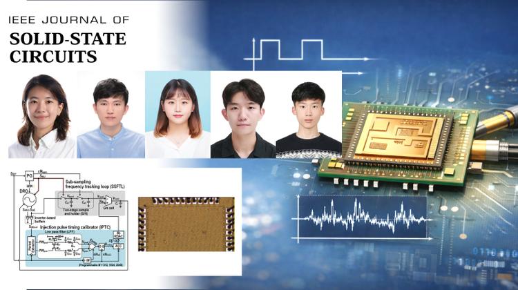
AI가 반도체 회로를 설계하고, 칩은 작동 중 스스로 신호 오차를 바로잡는다. UNIST 전기전자공학과 윤희인 교수 연구실 학생들이 이 같은 기술로 일주일 사이 삼성전자와 정보통신기획평가원(IITP) 상을 잇달아 받았다. 김성진 석·박사통합과정생은 지난달 19일 열린 삼성전자 DS부문 산학협력 교류회에서 ‘산학협력 우수 논문상’을 받았다. 삼성전자와 산학협력을 진행하는 국내 11개 대학과 미국 스탠퍼드대 교수진 등 총 1,177명이 참가한 행사다. 수상 논문은 ‘강화학습 기반 물리적 레이아웃을 포함한 LC-VCO 자동 설계 프레임워크(A Framework of Automated LC-VCO Design with Physical Layout Based on Reinforcement Learning)’다. LC 전압제어발진기(LC-VCO)는 5G·6G 통신 장비와 AI 반도체에 정확한 기준 주파수를 공급하는 핵심 회로다. 반도체가 일정한 박자에 맞춰 작동하도록 만드는 일종의 ‘전자 메트로놈’이다. 회로 변수 하나를 바꾸면 출력 주파수와 전력 소모, 잡음 특성이 함께 달라진다. 제조 공정이나 목표 주파수가 바뀔 때마다 숙련된 설계자가 수많은 변수 조합을 시뮬레이션하며 조정해야 했다. 복잡성과 비선형성이 커 AI 활용도 상대적으로 더뎠다. 김성진 학생은 이 과정을 자동화했다. 회로도를 만드는 단계에서는 강화학습으로 최적의 설계 변수 조합을 찾고, 실제 칩에 소자를 배치하고 배선을 연결하는 물리적 레이아웃 단계에서는 경사하강법 계열 알고리즘을 적용했다. 회로도와 칩 레이아웃을 따로 설계하던 기존 방식을 하나의 자동화 과정으로 연결한 것이다. 이 방법은 여러 반도체 공정과 주파수 대역에서 전력·잡음·주파수 성능을 종합한 우수한 성능지수(FoM)를 기록했다. 특정 공정에 맞춰 설계를 반복하는 작업을 줄여 칩 개발 기간과 비용을 낮출 수 있다. 장기적으로는 아날로그·RF 설계 인력 부족을 보완하고 기존 회로를 차세대 공정으로 옮기는 시간도 단축할 것으로 기대된다. 김성진 학생은 “뚜렷한 성과가 보이지 않을 때도 회로 설계 자동화가 재미있어 연구를 계속했다”며 “많은 설계자의 관심을 받게 돼 기쁘다. 앞으로도 즐겁고 건강하게 연구하며 설계 자동화 분야에 기여하겠다”고 말했다. 일주일 뒤인 8월 26일에는 남현준·안효경·안창민 석·박사통합과정생이 ‘ICT 챌린지 2026’에서 IITP 원장상을 받았다. 세 학생은 ‘ACELAB’팀명으로 참가해 ‘Injection-locking 기반 저스퍼 클록 생성기’를 선보였다. 클록은 반도체 내부의 수많은 연산이 같은 박자에 맞춰 이뤄지도록 하는 신호다. 주입 동기화(injection-locking)는 외부 기준 신호를 발진기에 넣어 주파수를 맞추는 기술로, 적은 전력으로 정밀한 클록을 만들 수 있다. 하지만 신호를 주입하는 과정에서 기준 주파수 주변에 불필요한 신호인 스퍼(spur)가 생기는 문제가 있었다. ACELAB팀은 스퍼가 가장 작아지는 신호 주입 시점을 회로가 스스로 찾도록 설계했다. 반도체 제조 공정과 전압, 온도가 달라져 최적 시점이 바뀌면 보정 회로가 새로운 시점을 탐색해 다시 조정한다. 복잡한 외부 제어 장치 없이도 신호의 시간 흔들림인 지터(jitter)와 레퍼런스 스퍼를 동시에 낮춘 것이 특징이다. 이 기술은 정밀한 클록이 필요한 AI 가속기와 고속 통신 장비, 차세대 시스템온칩(SoC)에 활용할 수 있다. 연구팀은 앞으로 반도체 공정과 동작 주파수별 클록 설계자산(IP)으로 개발해 국내 시스템반도체의 성능과 설계 경쟁력을 높일 계획이다. 과학기술정보통신부가 주최하고 IITP와 대학정보통신연구센터협의회가 주관한 이번 대회에는 전국 39개 대학, 84개 연구센터에서 206개 팀, 618명이 참가했다. 예선을 통과한 32개 팀 가운데 16개 팀이 수상했고, ACELAB팀을 포함한 5개 팀이 IITP 원장상에 선정됐다. 기술 성능뿐 아니라 시장성과 사업화 가능성도 인정받았다. 수상팀은 부상으로 중국 하이테크 페어 ‘CHTF 2026’ 해외연수 기회도 얻었다. ACELAB팀은 “연구의 기술성과 가능성을 인정받아 기쁘다”며 “앞으로도 실제 산업에 기여할 수 있는 반도체 기술을 개발하겠다”고 소감을 전했다.

원자력공학과, ‘원자력 안전규제라운드테이블’ 개최

연구 2026년 08월 21일 금요일

몸 뒤척여도 체내 의료기기 안정적으로 충전하는 무선충전 기술 개발

몸을 이리저리 뒤척이거나 걷고 숨을 쉬는 등 움직이는 와중에도 체내에 삽입된 의료기기를 안정적이고 효율적으로 무선 충전할 수 있는 새로운 기술이 개발됐다. UNIST 전기전자공학과 변영재 교수팀은 체내 삽입형 의료기기가 환자의 움직임이나 작동 상태가 달라져도 전압을 일정하게 유지하고, 필요한 만큼만 전력을 받아 전력 손실과 발열 가능성을 줄일 수 있는 무선 충전 기술을 개발했다고 29일 밝혔다. 체내에 삽입된 의료기기는 치료나 통신 기능을 작동할 때와 대기할 때 사용하는 전력이 달라진다. 체외 충전 송신부가 몸속 수신부에 전력이 필요한 상황인지를 알아내 전력 공급 모드와 저전력 모드를 오가면, 필요한 때에만 충분한 전력을 보내 불필요한 전력 소모를 줄일 수 있다. 연구팀이 개발한 기술은 환자가 몸을 움직여도 수신부의 상태를 정확히 판단해 송신 출력을 조절할 수 있는 ‘적응형 모드 전환 기술’이다. 무선 충전은 전기를 보내는 송신 코일과 전기를 받는 수신 코일 사이의 거리와 정렬 상태가 중요한데, 몸이 움직이면 송신부에서 측정되는 신호가 달라진다. 전력이 필요 없는데도 계속 보내 열이 나고 전기가 낭비되거나 반대로 전력이 필요한데도 저전력 모드에 머물면 의료기기가 제대로 작동하지 않거나 멈출 수 있게 된다. 개발된 기술은 신호의 절대적인 크기 대신 수신부의 상태가 바뀌는 순간 나타나는 신호 변화와, 짧은 확인 신호를 보낸 뒤 수신부 상태에 따라 달라지는 반응을 각각 읽어 전력 공급 모드에서는 저전력 모드로, 저전력 모드에서는 다시 전력 공급 모드로 정확히 넘어갈 수 있도록 했다. 또 몸속 수신부에는 공급 전압을 빠르게 조절하는 ‘전압 경주형 히스테리시스 제어기(VRHC)’ 기술도 적용했다. 의료기기는 일정한 전압에서 작동하기 때문에 전압이 크게 흔들리면 제대로 작동하지 않거나 멈출 수 있다. 이 제어 기술은 전압을 기준 전압과 직접 비교하는 대신, 전압 정보를 같은 시점에 출발한 신호들이 회로를 지나 나오는 시간 차이로 바꿔 읽어내기 때문에 전압이 기준을 벗어났는지를 빠르게 판단할 수 있다. 실험 결과, 송·수신 코일 사이의 거리를 7㎜에서 20㎜까지 바꾸며 검증했을 때도 우수한 성능을 입증했다. 의료기기 사용 전류가 6mA에서 16mA로 급증하는 상황에서도 출력 전압은 3.3V를 안정적으로 유지했으며, 전압 출렁임(리플)은 18mV 수준에 그쳤다. 체외 송신부에서 체내 수신부 출력까지 전달되는 종단 간 효율은 최고 69.1%를 기록해, 적응형 모드 전환 기술을 적용하지 않았을 때보다 효율이 최대 51.3%포인트 상향됐다. 변영재 교수는 “이번 기술은 환자가 움직여 코일 위치가 달라져도 필요한 전력만 안정적으로 전달해 체내 의료기기의 배터리 교체 수술 부담을 줄이고, 장기 사용과 치료 편의성을 크게 끌어올릴 것”이라고 설명했다. 이번 연구에는 신성민·권성빈 연구원이 공동 제1저자로 참여했다. 연구 수행은 과학기술정보통신부 정보통신기획평가원의 지원을 받아 이뤄졌으며, 연구 결과는 회로·시스템 분야 국제학술지 ‘IEEE 트랜잭션스 온 서킷츠 앤드 시스템스 원: 레귤러 페이퍼스(IEEE Transactions on Circuits and Systems I: Regular Papers)’ 에 6월 19일 게재됐다.

원자력공학과, ‘원자력 안전규제라운드테이블’ 개최

연구 2026년 08월 19일 수요일

‘로직인메모리’ 반도체 효율 높이는 자동 설계 기술 개발

데이터를 별도의 연산장치로 보내지 않고도 메모리에서 직접 처리하는 로직인메모리 반도체의 성능을 높일 수 있는 설계자동화 기술이 개발됐다. 이 기술을 적용하면 전체 동작 횟수를 기존보다 평균 20% 가까이 줄일 수 있다. 데이터 이동이 성능의 발목을 잡는 인공지능(AI)과 빅데이터 처리 분야의 저전력·고성능 반도체 설계에 활용될 것으로 기대된다. UNIST 전기전자공학과 박희천 교수팀은 메리스터 ‘로직인메모리’ 반도체의 회로 배치와 연결 경로를 자동으로 최적화하는 기술을 개발했다고 26일 밝혔다. 컴퓨터는 데이터 저장 메모리와 연산 담당 프로세서가 분리돼 있다. 데이터가 메모리와 프로세서 사이를 오가는 데 시간과 전력이 소모되면서, 프로세서의 빠른 연산 성능을 데이터 전송 속도가 미처 따라가지 못하는 ‘메모리 벽(memory wall)’이 발생하게 된다. 로직인메모리(Logic-in-Memory, LiM)는 메모리가 데이터 저장과 논리 연산을 함께 맡아 이러한 데이터 이동을 줄이는 반도체다. 연구팀이 개발한 기술은 멤리스터 소자가 바둑판처럼 배열된 형태의 로직인메모리에서 연산 배치와 데이터 이동 경로 설계를 자동화하는 기술이다. 멤리스터는 저항 상태에 따라 0과 1의 데이터를 저장하는 소자다. 설계 과정에서 바둑판 내의 특정 구역들을 연산을 수행할 '계산 블록'으로 할당하고, 각 블록에서 산출된 결과값을 다음 연산 단계를 위해 어느 물리적 경로로 보낼지를 컴퓨터 알고리즘이 자동으로 탐색하여 최적화하게 된다. 이 기술은 기존 기술들과 달리 가로와 세로 방향에서 모두 여러 연산을 동시에 수행할 수 있다. 순차적으로 처리해야 할 연산이 줄어 전체 동작 횟수를 낮추고, 제한된 멤리스터 공간도 더 효율적으로 활용할 수 있게 된다. 기존 기술은 계산 블록의 세로 방향 정렬까지 고려하지 않아, 주로 가로 방향의 연산만 동시에 처리할 수 있었다. 또 연산이 끝난 불필요한 데이터를 지우고 사용 중인 중간 결과물들을 한쪽으로 정렬해 낭비되는 면적을 최소화하는 규칙도 자동 설계 알고리즘에 반영했으며, 수학적 경로 탐색 기법이 적용돼 가장 효율적인 계산 결과 이동 경로를 탐색해 낼 수 있다. 이 기술로 설계한 반도체는 최고 수준 기술보다 전체 사이클 동작 횟수가 평균 19.6% 줄었다. 같은 계산을 끝낼 때까지 반도체가 작동해야 하는 횟수가 그만큼 줄었다는 뜻이다. 또 메모리 공간을 엄격하게 제한한 조건에서도 기존 기술이 배치하지 못한 회로까지 모두 배열 안에 넣을 수 있었다. 연구팀은 “회로를 메모리에 단순히 욱여넣는 것이 아니라, 병렬 연산이 가능하도록 정렬해 배치하는 것이 인메모리 컴퓨팅 성능을 좌우한다”며 “좁은 면적 제약에서도 안정적으로 동작하는 자동 설계 기술이라는 점에서 의미가 크다”고 설명했다. 이번 연구는 UNIST 김익겸 연구원이 제1저자, 김민홍 연구원이 제2저자로 참여했고, 박희천 교수가 교신저자로 연구를 이끌었다. 연구 결과는 반도체 설계자동화 분야 권위 학술지인 ‘IEEE 집적회로 및 시스템 설계자동화 회보(IEEE TCAD, Transactions on Computer-Aided Design of Integrated Circuits and Systems)’에 2026년 6월 2일 온라인(Early Access) 공개됐다. 연구는 한국연구재단(NRF)과 정보통신기획평가원(IITP)의 지원으로 수행됐으며, 칩 설계 도구는 반도체설계교육센터(IDEC)의 지원을 받았다.

원자력공학과, ‘원자력 안전규제라운드테이블’ 개최

연구 2026년 08월 05일 수요일

반도체 잉크 발라 6G·우주통신용 고주파 스위치 만든다!

잉크 상태의 원료를 기판에 발라 만든 이차원 반도체 박막을 기반으로 하는 통신용 반도체 소자가 새롭게 개발됐다. UNIST 전기전자공학과 김명수 교수팀은 용액공정으로 만든 이황화몰리브덴(MoS₂) 박막을 이용해 67기가헤르츠(GHz) 대역까지 작동하는 저전력·고성능 고주파 스위치를 개발했다고 22일 밝혔다. RF(고주파) 스위치는 스마트폰, 위성통신, 레이더, 무선기지국, 자율주행 통신 장비 등에서 고주파 신호의 흐름을 연결하거나 차단하는 필수 반도체 소자다. 특히 6G와 우주통신처럼 많은 안테나와 주파수 채널을 동시에 사용하는 시스템에서는 낮은 삽입손실과 높은 절연 성능, 낮은 소비전력의 3박자를 갖춘 스위치가 필요하다. 연구팀이 개발한 스위치는 병렬형 구조에서 67GHz 기준 삽입손실 0.1데시벨(dB) 미만, 절연도 35dB 이상의 성능을 기록했다.1초에 670억 번 진동하는 고주파 신호가 들어왔을 때 입력 신호의 약 98%를 거의 손실 없이 통과시키고, 스위치를 껐을 때 새는 신호는 0.03% 이하로 억제했다는 의미다. 일반적으로 주파수가 높아질수록 신호 손실과 누설이 커지기 쉬운데, 6G와 위성통신에 쓰이는 밀리미터파 대역에서도 낮은 삽입손실과 높은 절연 성능을 동시에 유지한 것이다. 신호의 통과와 차단 성능을 종합한 지표인 작동 저항과 차단 정전용량의 곱도 약 0.8펨토초로, 1펨토초보다 작은 ‘서브 펨토초급’ 성능을 달성했다. 또 스위치를 켜거나 끈 상태를 유지하기 위한 대기전력 소모도 없다. 이 스위치는 이황화몰리브덴 반도체 박막을 금속 전극 사이에 넣은 구조로, 전압을 가하면 전극에서 나온 이온이 통로를 형성하며 스위치를 켜는 방식이라, 전원을 꺼도 이미 만들어진 통로가 유지되는 덕분이다. 특히 스위치에 들어간 이황화몰리브덴 박막은 용액공정으로 만들어져 제조가 간단하고 넓은 면적에 적용하기도 쉽다. 용액공정은 반도체 소재를 액체 상태로 만든 뒤 기판에 직접 바르는 방식으로, 박막을 별도로 성장시켜 떼어 옮기는 복잡한 전사 과정이 필요 없다. 일반적으로 용액공정에서는 황 원자 자리가 비는 결함이 발생하기 쉬운데, 반도체 스위치에서는 이 황 빈자리가 구리 이온의 이동 경로를 일정하게 잡아주는 역할을 해 오히려 내구성을 향상시키는 것으로 분석됐다. 실제로 기계적으로 떼어낸 이황화몰리브덴 박막으로 만든 스위치는 반복 작동 수명이 약 100회에 그쳤지만, 용액공정 박막을 쓴 스위치는 2,000회 반복 작동에도 성능을 유지했다. 연구팀은 개발한 스위치를 실제 통신 회로에도 적용해 성능을 검증했다. 하나의 안테나를 송신기와 수신기에 번갈아 연결하는 회로와, 여러 안테나에서 나오는 전파의 타이밍을 조절해 빔의 방향을 바꾸는 위상변위기를 제작해 정상 작동을 확인했다. 위상변위기는 여러 안테나가 전파를 내보내는 시점을 조절해 빔의 방향을 바꾸는 회로로, 안테나 자체를 움직이지 않고도 전파 방향을 빠르게 바꿀 수 있어 이동 위성이나 드론처럼 위치가 계속 달라지는 대상을 빠르게 추적할 수 있다. 김명수 교수는 “복잡한 전사 공정이 필요 없는 용액공정 제조 이차원 반도체 물질로, 밀리미터파 대역에서도 신호 손실은 낮고 차단 성능은 높은 RF 스위치를 개발했다”며 “전원을 꺼도 스위치 상태가 유지돼 대기전력이 들지 않는 만큼, 6G와 위성통신, 레이더, 방산용 전파 제어 시스템을 더 작고 에너지 효율적으로 만드는 데 활용할 수 있을 것”이라고 설명했다. 이번 연구는 과학기술정보통신부 한국연구재단, 정보통신기획평가원의 우수신진연구, Space-K BIG 프로젝트, InnoCORE 사업, 지역지능화혁신인재양성사업의 지원을 받아 수행되었으며, 연구 결과는 세계적 학술지 ‘네이쳐 커뮤니케이션즈(Nature Communications)’에 6월 18일 온라인 공개됐다.

원자력공학과, ‘원자력 안전규제라운드테이블’ 개최

연구 2026년 07월 15일 수요일

"부정맥부터 가스 위험 감지까지"… 패치 안에서 바로 판단하는 온칩 AI 기술 개발

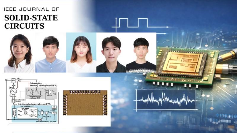
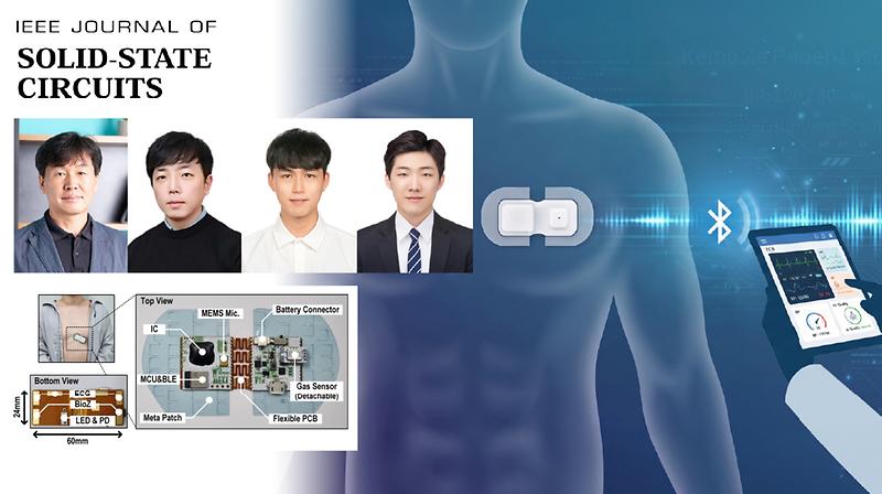
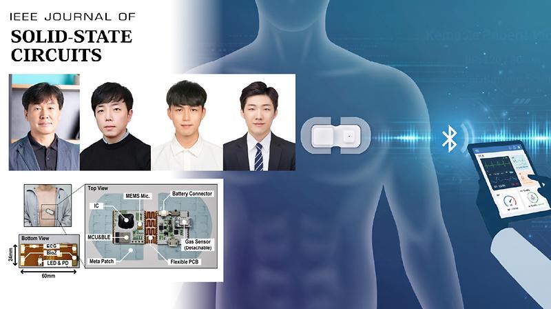
심전도, 혈압과 같은 생체 신호와 대기 가스 정보를 동시에 분석해 질병이나 위험 상황을 알 수 있는 부착형 패치가 개발됐다. 대기오염에 민감한 기저질환자, 노약자의 맞춤형 건강관리나, 밀폐 공간 작업자 모니터링에 쓸 수 있는 기술이다. UNIST 전기전자공학과 김재준 교수팀과 기계공학과 정훈의 교수팀은 심전도, 혈압과 같은 생체 정보와 함께 주변 유해 가스를 동시에 감지해 심혈관 질병이나 이상 상태를 즉시 판별할 수 있는 가슴 부착형 패치를 개발했다고 30일 밝혔다. 이 패치는 아날로그 연산 기반 온칩 인공지능 회로를 이용해 센서가 측정한 측정 데이터를 외부로 보내지 않고 패치 내부에서 바로 분석해 낸다. 판단 결과를 블루투스를 통해 외부로 전송할 수 있어, 관리자가 여러 명을 동시에 원격으로 모니터링할 수 있다. 무거운 원시 데이터(Raw data) 대신 칩이 자체 판단한 가벼운 결괏값만 전송하므로 통신 끊김과 지연은 최소화하고, 통신 자체에 드는 전력 소모를 줄였다. 또 광학 센서를 선택적으로 작동시키는 저전력 회로 설계 기술이 적용돼 한 번 충전으로 장시간 착용할 수 있다. 광학 센서는 혈류 정보를 얻는 역할을 하는데, 기기에서 전력 소모가 가장 많다. 연구진은 심전도 신호 주기에 맞춰 센서를 켜고 끄는 저전력 기술(RPT-PW)을 적용한 결과, 기존 대비 해당 센서부의 전력 소모가 약 83%나 줄었다. 개발된 패치는 고혈압이나 부정맥을 90% 이상의 정확도로 진단했으며, 유해가스 혼합물 분류 실험에서, 92.46%의 진단 정확도를 기록했다. 패치 접착면에 미세 구조 기술이 적용돼, 거친 피부에도 잘 접착되며, 패치를 떼어낼 때는 한쪽 방향으로 쉽게 떨어져 잔여물이 남지 않는다. UNIST 전기전자공학과 조상현 연구원과 김현중 연구원이 제1저자로 참여한 이번 연구는 회로 설계 분야 최고 학술지인 ‘IEEE 저널 오브 솔리드 스테이트 서킷스(Journal of Solid-State Circuits)’ 7월호에 정식 게재될 예정이다. 한편 연구진이 공동 창업한 ㈜앤빅스랩(Anvix Lab)은 개발된 기술을 이전받아 온칩 AI 기반의 차세대 바이오일렉트로넥스 패치 플랫폼 상용화를 추진 중이다. 이번 연구는 산업통상부, 교육부, 과학기술정보통신부의 지원을 받아 수행되었다.

원자력공학과, ‘원자력 안전규제라운드테이블’ 개최

연구 2026년 07월 01일 수요일

우주·6G 통신 칩 전력 줄일 반도체 소자 개발

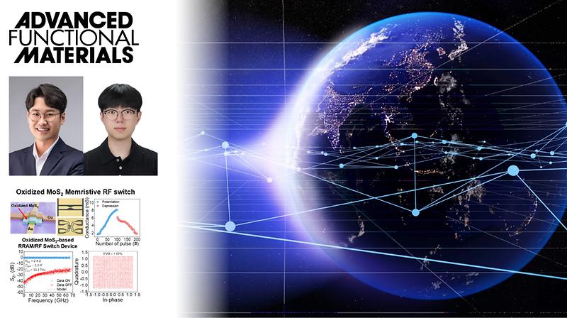
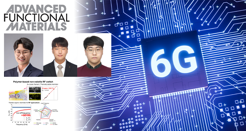
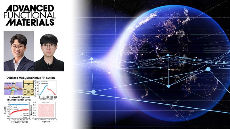
전력과 공간 제약이 큰 우주 위성통신과 6G 통신에서 데이터를 더 적은 전력으로 처리할 수 있는 반도체 소자가 개발됐다. UNIST 전기전자공학과 김명수 교수팀은 산화 2차원 반도체 소재를 기반으로 한 다기능 멤리스터 반도체 소자를 개발했다고 22일 밝혔다. 이 멤리스터 반도체 소자는 통신 고주파 신호의 길을 여닫는 RF 스위치와 연산 소자로 모두 쓸 수 있다. 덕분에 칩 면적을 작게 만들 수 있고, 신호를 다른 회로로 옮기고 변환하는 과정에서 드는 전력과 지연도 낮출 수 있다. 또 한 번 상태를 바꿔 두면 전원을 끊어도 켜짐·꺼짐 상태가 유지돼, 대기 전력 소모가 없다. 태양광 등 제한된 에너지만으로 작동해야 하는 위성 통신 장비나 6G 기지국처럼 전력과 공간 제약이 극심한 시스템에 이 기술이 적합한 이유다. 연구팀은 2차원 반도체 소재인 이황화몰리브덴(MoS2)을 400℃에서 산화시켜 이 같은 소자를 만들었다. 산화 이황화몰리브덴은 전압을 걸었을 때 저항이 낮아져 스위치가 켜지고, 전압을 반대 방향으로 걸면 저항이 높아져 스위치가 꺼지게 된다. 별도로 전압을 걸어주지 않는 한 저항 상태가 유지되기 때문에 대기 전력이 필요 없게 된다. 이 단일 소자를 바둑판처럼 배열한 회로로는 연산을 할 수 있다. 각 소자의 저항(전도도)이 행렬 계산에서 가중치 역할을 할 수 있기 때문이다. 통신에서는 여러 안테나에서 들어온 신호가 서로 섞여 있어서 원하는 신호를 골라내려면 각 신호에 알맞은 비율을 곱해 더하는 행렬 연산이 필요하다. 기존에는 이 계산을 위해 아날로그 고주파 신호를 디지털 신호로 바꾸고, 별도의 프로세서 회로로 데이터를 옮겨 처리해야 했다. 실험에서 이 소자를 한 번 켜거나 끄는 데 드는 스위칭 에너지는 140pJ(피코줄, 10⁻12)로 매우 낮았고, 상태를 바꾸는 동작 전력 역시 1mW(밀리와트) 이하로 측정됐다. 한 번 바뀐 저항 상태는 4만 초 이상 유지되는 비휘발성과 1,000회 이상 반복 동작에서도 안정성을 보였다. 초고속 통신에 쓰이는 고주파 대역의 스위칭 성능은 실험에서 67GHz까지 검증됐다. ON 저항과 OFF 커패시턴스를 기반으로 계산한 차단주파수는 33.2THz에 달했다. 연구팀은 소자 회로의 연산 성능도 시뮬레이션으로 검증해, 1024-QAM 신호 복조와 MIMO 신호 복원이 이뤄짐을 확인했다. 제1저자인 손주호 연구원은 “기존 상용 반도체 고주파 스위치는 지속해서 대기 전력을 소모하고 고주파 대역에서 신호 손실이 발생하는 문제가 있었는데, 이 소자는 이러한 한계를 근본적으로 해결한 기술”이라며 “차세대 상변화 메모리(PCM)나 MEMS와 비교해도 각각 에너지 소모 효율과 초고주파 동작 속도 및 초소형화 측면에서 경쟁력을 갖춘 기술”이라고 설명했다. 김명수 교수는 “이번 연구는 산화 2차원 반도체 기반 멤리스터가 고성능 밀리미터파 RF 스위치뿐 아니라 6G 신호처리에 필요한 인메모리 행렬 연산 하드웨어로도 활용될 수 있음을 보여준 사례”라며, “비휘발성·저전력·고주파 특성을 동시에 확보한 만큼, 위성통신, 레이더, 방산용 전파 제어 시스템, 6G RF 프론트엔드의 소형화와 에너지 효율 향상에 기여할 수 있을 것”이라고 설명했다. 이번 연구는 과학기술정보통신부 한국연구재단, 정보통신기획평가원의 우수신진연구, Space-K BIG 프로젝트, 지역지능화혁신인재양성사업의 지원을 받아 수행됐으며, 연구 결과는 세계적 학술지 ‘어드밴스드 펑셔널 머티리얼즈(Advanced Functional Materials)’에 6월 6일 온라인 공개됐다. (끝)

원자력공학과, ‘원자력 안전규제라운드테이블’ 개최

대학소식 2026년 06월 09일 화요일

UNIST 전기전자공학과, 우주항공청 ‘Space-K BIG 프로젝트’ 선정

UNIST 전기전자공학과 연구팀이 우주항공청(KASA)이 주관하는 ‘2026년도 Space-K BIG 프로젝트 사업’ 인공위성·우주임무보증 분야 신규 과제 수행 기관으로 최종 선정됐다. Space-K BIG 프로젝트는 우주 분야 기술개발 역량과 인력양성 기반을 갖춘 대학을 연구센터로 지정해 기초·원천기술을 축적하고, 전문 인재를 체계적으로 길러내는 우주항공청의 핵심 사업이다. 이번 선정으로 UNIST 연구팀은 2030년 12월까지 연구를 수행한다. 총 57억 원의 정부출연금을 지원받아 임무 주도형 초저궤도 위성 플랫폼 개발과 우주 특화 인재 양성에 속도를 낸다. 이번 대형 과제는 전기전자공학과 변강일 교수가 연구책임자를 맡았다. 김명수, 이훈, 박진석, 최민호, 감동윤, 한가원, 정재용 교수가 함께 참여해 학과의 연구 역량을 모은다. 선정된 연구개발과제는 ‘임무 주도형 초저궤도 위성 융복합 플랫폼 원천기술 확보 및 글로벌 인재 양성’이다. 연구팀은 우주 임무에 필요한 핵심 소자와 부품, 플랫폼 기술을 아우르는 융복합 연구를 추진한다. 주요 연구 방향은 세 가지다. 먼저 RF, AI 반도체, 광·전자 소자가 극한 우주 환경에서도 안정적으로 작동할 수 있도록 신뢰성을 확보한다. 이어 저궤도 위성에 적용할 수 있는 국산 COTS, 즉 상용 완제품을 개발하고, 실제 운용을 통해 우주 헤리티지 확보에 나선다. 또 초저궤도 위성 융합 플랫폼을 구축해 미래 우주 임무에 투입할 수 있는 실전형 기술 기반을 마련한다. 인재 양성도 핵심 축이다. UNIST 연구팀은 국내외 우주항공 분야 기업, 정부출연연구소와 산·학·연 협력 생태계를 꾸려 공동 연구를 수행할 계획이다. 실습과 공동 프로젝트를 연계한 교육 프로그램을 운영해 연구개발과 교육이 맞물려 돌아가는 선순환 체계도 구축한다. 연구책임자 변강일 교수는 “이번 Space-K BIG 프로젝트 선정을 계기로 UNIST가 대한민국 초저궤도 위성 원천기술 연구를 선도하고, 세계적 수준의 우주 특화 인재를 배출할 기반을 마련했다”며 “참여 교수진의 전문성과 협력 기업의 혁신 기술을 결합해 미래 우주 산업에 실질적으로 기여할 성과를 내겠다”고 말했다.

원자력공학과, ‘원자력 안전규제라운드테이블’ 개최

커뮤니티 2026년 06월 05일 금요일

윤성환 교수, ‘디지털인재양성 공로’ 과기정통부 장관 표창

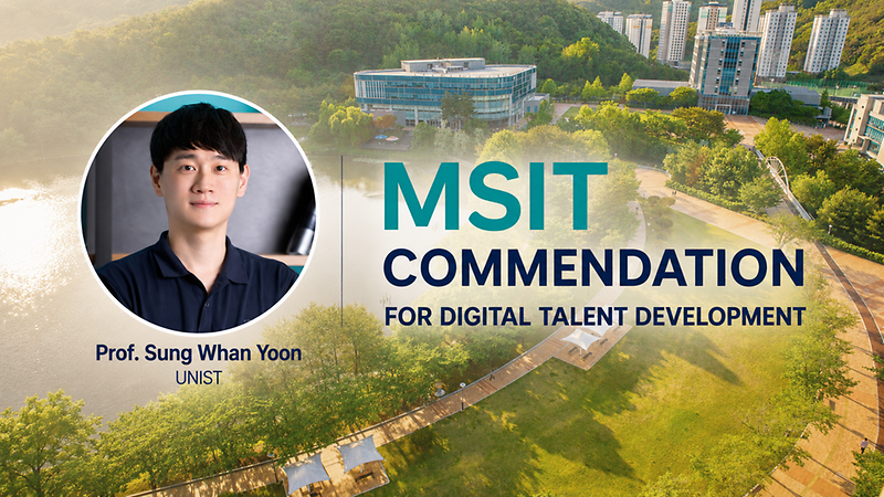
윤성환 교수(인공지능대학원·전기전자공학과)가 디지털인재양성 공로로 부총리 겸 과학기술정보통신부 장관 표창을 수상했다. AI 기술을 제조 현장 교육과 공정 혁신으로 연결해 온 점을 인정받았다. AI를 공장에 적용할 때 가장 큰 변수는 현장이다. 연구실에서 학습한 데이터와 실제 설비에서 들어오는 데이터는 같지 않다. 원료 상태, 장비 조건, 운전 방식, 데이터 품질이 바뀌면 모델의 판단도 흔들릴 수 있다. 제조업에서는 이런 오류가 곧 생산 손실이나 안전 문제로 이어진다. 윤 교수는 이런 한계를 줄이는 ‘강건한 인공지능’ 학습 알고리즘을 개발해 왔다. 강건한 AI는 학습 때 보지 못한 환경 변화가 생겨도 안정적으로 작동하는 기술이다. 정해진 조건에서 높은 정확도를 내는 데 그치지 않고, 실제 산업 현장에서 신뢰할 수 있는 판단을 내리도록 만드는 것이 핵심이다. 그의 연구 역량은 딥러닝 분야 대표 학술대회인 ‘International Conference on Learning Representations(ICLR 2025)’에서 높이 평가됐다. 윤 교수는 AI 기반 최적화 기술인 강화학습 모델의 안정성을 높인 연구로 구두 발표 논문에 선정됐다. ICLR 구두 발표는 제출 논문 가운데 상위 2% 수준의 연구에 주어지는 성과다. 강화학습은 AI가 여러 선택을 시도하고 결과를 학습해 더 나은 결정을 찾아가는 기술이다. 제조 현장에서는 설비 운전 조건을 조정하거나 생산 공정을 효율화하는 데 활용될 수 있다. 다만 공장에서는 한 번의 잘못된 결정도 비용과 안전 리스크로 이어질 수 있다. 윤 교수의 연구는 강화학습이 불확실한 현장 조건에서도 흔들리지 않도록 신뢰성을 높였다는 점에서 주목받았다. 논문으로 검증한 기술은 울산과 동남권 제조업 교육 현장으로도 옮겨졌다. 윤 교수는 UNIST 부임 이후 산업체 재직자 대상 AI 교육 설계와 운영에 참여했다. 교육은 이론 강의가 아니라 현장 문제 해결에 맞춰졌다. 재직자들이 공정에서 겪는 문제를 제시하고, 이를 AI 실습 과제로 바꾸는 방식이었다. 공장 단위 생산·가공 설비에 강화학습 기반 최적화 기법을 적용한 사례도 만들었다. 공정의 안전성과 안정성을 유지하면서 설비 운영을 개선하는 접근이다. AI를 배우는 데서 끝내지 않고 실제 업무 변화로 이어지게 한 점이 이번 표창의 주요 배경으로 꼽힌다. 그는 현재 UNIST가 수행 중인 국가 주요 AI 연구 과제인 ‘AI스타펠로우십’에서 신진 프로젝트 리더로도 참여하고 있다. SK에너지와 협력해 석유화학 산업을 포함한 공정 프로세스에 적용 가능한 강건한 제조AI 원천기술을 개발하고 있다. 윤 교수는 “인공지능이 산업 현장에서 실제로 쓰이려면 높은 성능만으로는 부족하다”며 “환경이 달라져도 안정적으로 작동하는 강건한 AI 원천기술을 발전시키고, 이를 제조 현장의 문제 해결과 디지털 인재 양성으로 이어가겠다”고 소감을 밝혔다.

원자력공학과, ‘원자력 안전규제라운드테이블’ 개최

연구 2026년 05월 30일 토요일

6G 통신과 배터리 잡을 ‘카멜레온 맥신’ 개발

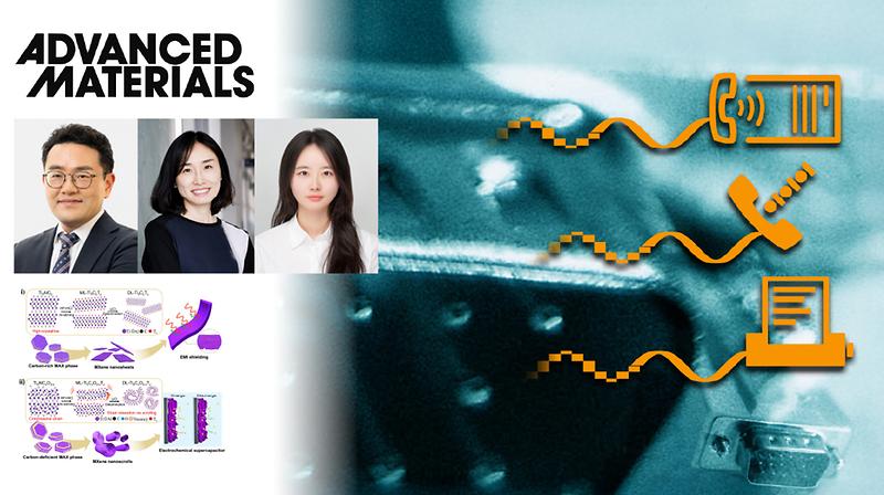
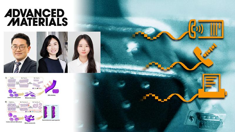
* 본 보도자료는 한국연구재단 주관으로 작성되었습니다. (바로 가기) □ 국내 연구진이 탄소 조성 제어로 꿈의 신소재 ‘맥신(MXene)*’을 정밀 제어해 초고주파 EMI(Electromagnetic Interference Shielding) 차폐**와 고속 에너지 저장 성능을 세계적 수준으로 끌어올려 주목을 받고 있다. * 맥신(MXene) : 금속과 탄소층이 교대로 쌓인 2차원 나노소재로, 전기전도성이 뛰어나고 다양한 화합물 설계가 가능해 배터리·반도체·센서 분야의 꿈의 신소재로 불림. ** 초고주파 EMI(Electromagnetic Interference Shielding) 차폐 : 차세대 6G 통신, 고해상도 차량용 레이다, 위성 통신 등에서 발생하는 고주파 영역의 전자파 간섭을 막아내는 핵심 기술. □ 한국연구재단(이사장 홍원화)은 울산과학기술원 권순용·최은미 교수 연구팀이 MAX 전구체*의 탄소 조성을 정밀 제어해 맥신의 구조와 기능을 합성 단계에서 선택적으로 설계하는 데 성공했다고 밝혔다. * MAX 전구체 : 맥신을 만들기 위한 전 단계의 초기 원료 물질(화합물) □ 이번 연구성과는 과학기술정보통신부와 한국연구재단이 추진하는 나노․소재기술개발사업의 지원으로 수행됐으며, 재료과학 분야 세계적 권위지인 ‘어드밴스드 머티리얼즈(Advanced Materials)’에 5월 18일 게재됐다. □ 6G 통신, 자율주행 레이더, 고집적 패키징 등 차세대 전자기기가 고주파 환경으로 빠르게 전환됨에 따라, 전자파 간섭으로 인한 오동작을 막아줄 초박막 차폐 기술의 필요성이 커지고 있다. ○ 그러나 기존 금속계 차폐재는 높은 차폐성에도 불구하고 무겁고 부식에 취약해, 유연·경량·초박막화를 동시에 요구하는 차세대 전자기기에는 제약이 있었다. 이러한 이유로 높은 전도도와 용액공정 적합성을 갖는 맥신 계열 소재가 대안으로 주목받고 있다. □ 최근 맥신의 전기적·구조적 특성을 근본적으로 제어하기 위한 전구체 수준의 조성·구조 설계가 핵심 기술로 주목받고 있다. 연구팀은 맥스 전구체의 탄소 조성을 정밀 제어하는 방법으로 맥신의 구조와 기능을 선택적으로 구현하는 데 성공했다. ○ 탄소가 풍부한 조건에서는 전기전도도가 우수한 평면 나노시트 구조가 형성되어, 100GHz 초고주파 대역에서 탁월한 전자파 차폐 성능과 뛰어난 굽힘 내구성을 나타냈다. ○ 반대로 탄소가 부족한 조건에서는 나노 스크롤 구조가 자발적으로 형성되어 이온 이동 통로가 확장되었으며, 이를 통해 고용량과 압도적인 수명 특성을 가진 고속 에너지 저장 성능을 확보했다. ○ 연구팀은 이번 연구 성과를 통해 전구체 조성 조절만으로 차폐용 평면 시트와 에너지 저장용 스크롤 구조를 하나의 플랫폼에서 맞춤형으로 설계할 수 있음을 입증했다. □ 박재은(제1저자) 연구원은 “평면 시트는 전자파 차폐에, 나노스크롤은 에너지 저장에 유리하다는 점을 실험적으로 입증해 하나의 소재 플랫폼에서 응용 방향을 나눠 설계할 수 있게 됐다”고 밝혔다. ○ 그리고 권순용 교수는 "지난해에는 질소 치환으로 맥신의 전도도와 광대역 차폐 성능을 끌어올렸다면, 이번에는 전구체 조성만으로 맥신 구조 자체를 설계하는 단계로 나아갔다”며, “초박막이면서도 100GHz 대역에서 높은 차폐 성능과 굽힘 내구성을 함께 보여, 차세대 6G·레이다 환경에 필요한 유연 차폐 소재 가능성을 확인했다”고 밝혔다.

원자력공학과, ‘원자력 안전규제라운드테이블’ 개최

연구 2026년 05월 14일 목요일

수개월 걸리던 반도체 설계, AI가 ‘단 하루’ 만에 끝낸다!

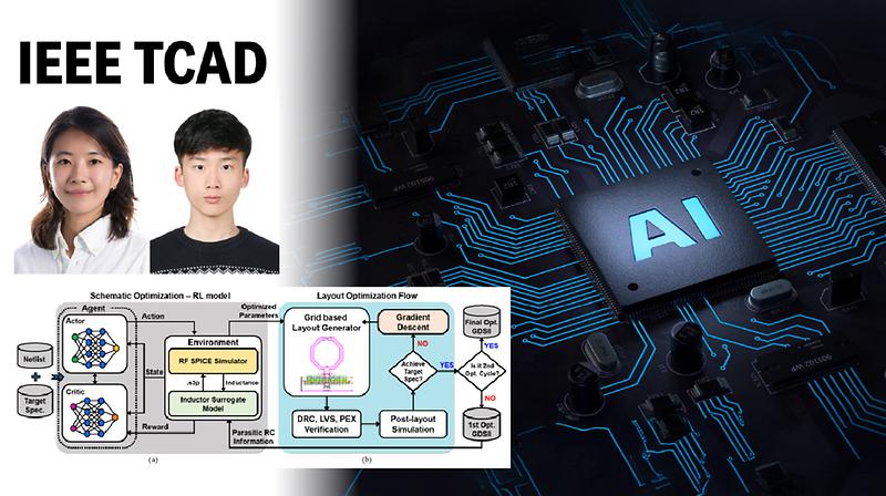
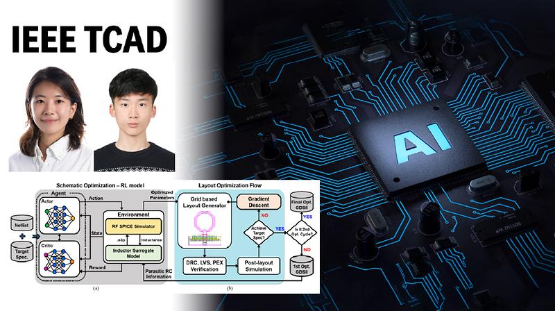
반도체 설계 전문가가 수주에서 수개월씩 걸려 작업하던 고성능 통신 반도체 회로 설계를 단 하루 만에 끝낼 수 있는 인공지능 기술이 개발됐다. UNIST 전기전자공학과 윤희인 교수와 경북대학교 송대건 교수팀은 통신 회로인 LC 전압제어 발진기(LC-VCO)를 회로 설계 단계부터 실제 칩에 넣는 물리적 레이아웃까지 자동으로 설계해주는 AI 모델을 개발했다고 5일 밝혔다. LC-VCO는 5G 같은 고속 통신 시스템에서 주파수를 만들어내는 반도체 회로다. 신호 잡음과 전력 소모를 줄이기 위해서는 인덕터, 트랜지스터 크기와 같은 변수를 잘 조합해 회로를 설계해야 하는데, 설계된 회로를 실제 칩 안으로 옮기기 위한 레이아웃 설계 단계에서는 회로 설계 단계의 조합이 깨지기 쉽다. 배선 굵기와 소자 배치에 따라 기생 효과가 더해지면서 주파수와 잡음 특성이 다시 달라질 수 있기 때문이다. 연구팀이 개발한 모델은 회로 설계와 레이아웃 설계를 통합해 최적화할 수 있다. 회로 설계 단계에서는 강화학습을 적용해 설계 변수들을 바꿔가며 목표 주파수와 성능을 만족하는 조합을 찾도록 했고, 실제 칩 구조가 결정되는 레이아웃 단계에서는 경사하강법을 이용해 배선 폭과 간격 같은 물리적 설계 변수를 성능이 개선되는 방향으로 반복적으로 보정하는 방식이다. 경사하강법은 현재 상태에서 성능이 더 좋아지는 방향을 따라 설계 값을 조금씩 조정해 최적의 조건을 찾아가는 최적화 기법이다. 연구팀은 “회로도 설계(Schematic)와 물리적 배치(Layout)를 개별적으로 최적화하던 기존 방식을 대신 AI가 두 단계를 통합적으로 관리하도록 한 기술”이라고 설명했다. 설계 과정에서 가장 시간이 오래 걸리는 인덕터는 딥러닝 기반 예측을 활용해 전체 설계 시간을 크게 줄였다. 설계자의 반복적인 전자기 시뮬레이션이 필요하던 작업을 단 몇 밀리초(ms) 만에 완료된다. 실험 결과, 기존의 자동 설계 방식이 약 119시간 소요되던 작업을 단 28.5시간 만에 완료해 설계 시간을 76% 이상 단축했다. 성능 지수(FoM) 또한 기존 연구 대비 월등히 우수한 결과를 보였다. 또 전이 학습이 적용돼 반도체 나노 공정 노드가 바뀌어도 기존에 학습한 내용을 바탕으로 설계를 이어갈 수 있다. 예를 들어 65nm 공정으로 학습한 AI는 40nm나 28nm 공정에서도 처음 학습에 필요했던 데이터의 약 10%만 추가로 활용해 설계를 수행할 수 있다. 공동 연구팀은 “5G·6G 통신과 AI 칩의 핵심 부품인 주파수 생성 회로의 성능은 높이면서 설계 비용은 크게 낮출 수 있을 뿐만 아니라 중장기적으로 반도체 설계 인력 부족 문제를 해결하고 차세대 공정으로의 전환 속도를 획기적으로 앞당길 수 있는 도구”라고 기대했다. 연구팀은 LC-VCO뿐만 아니라 다양한 아날로그/RF 회로 설계 자동화로 기술을 확장해 나갈 예정이다. 이번 연구는 UNIST 김성진 연구원과 경북대학교 이현수 연구원이 제1저자로 주도하였고 경북대학교 홍성민 연구원이 참여하였다. 연구 결과는 IEEE 반도체 회로 공학회에서 발행하는 권위 학술지인 ‘IEEE 집적회로 및 시스템 설계자동화(TCAD, Transactions on Computer-Aided Design of Integrated Circuits and Systems)’에 4월 3일 온라인 공개됐다. 연구는 과학기술정보통신부와 한국연구재단(NRF), 교육부(BK21 Four), 산업통상자원무(MOTIE), 반도체설계교욱센터(IDEC), 삼성전자, ㈜액시온 등의 지원 및 과기정통부와 정보통신기획평가원(IITP)의 '지역지능화혁신인재양성사업'의 지원으로 수행되었다.

원자력공학과, ‘원자력 안전규제라운드테이블’ 개최

대학소식 2026년 03월 13일 금요일

UNIST 양자나노팹 개소… "울산에 국가 양자 인프라"

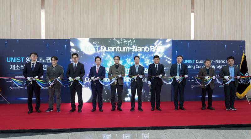
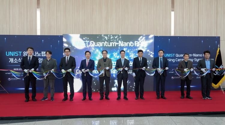
대한민국 양자기술 경쟁력 강화를 위한 국가 핵심 연구 인프라가 UNIST에 들어섰다. 13일, 총 300억 원 규모의 국가 양자 소자 개발 시설인 ‘UNIST 양자나노팹(Quantum-Nano FAB)’이 문을 열었다. 이날 108동 1층에서 열린 개소식·심포지엄에서는 양자 소자 설계부터 제작·분석·검증·실증까지 전 과정을 한곳에서 수행할 수 있는 원스톱 자율사용 연구 환경이 공개됐다. UNIST 양자나노팹은 과학기술정보통신부와 정보통신기획평가원(IITP)이 지원한 두 개 사업으로 조성됐다. 양자 소자 설계·제작·분석·검증·실증까지 이어지는 연구 전주기를 한 공간에서 수행할 수 있도록 공정 장비와 분석 체계를 통합한 것이 특징이다. 이 시설은 UNIST가 18년간 운영해 온 개방형 나노팹을 기반으로 구축됐다. UNIST 나노팹은 전국 60여 개 기관이 공동 활용하는 연구 공정을 연간 3만3000여 건 수행하고 매년 800여 명의 자율사용 연구자를 배출해 왔다. 여기에 양자 공정 특화 장비와 전담 지원 체계를 추가하면서 ‘UNIST 양자나노팹’으로 기능을 확장했다. 이번 양자나노팹 개소로 UNIST는 기존 나노 공정 중심 연구 환경에서 양자 소자 공정까지 아우르는 연구 거점으로 확대된다. 이를 바탕으로 울산을 양자·반도체 산업을 연결하는 동남권 혁신 허브로 육성한다는 계획이다. 산업 수도 울산은 자동차·조선·석유화학을 중심으로 발전해 왔지만 첨단 반도체 분야 기반은 상대적으로 부족했다. UNIST는 반도체대학원 설립과 나노팹 구축을 통해 산업 구조 전환의 토대를 마련해 왔으며, 이번 양자나노팹 개소를 계기로 울산을 미래 기술 표준을 창출하는 하이테크 연구·산업 도시로 발전시킨다는 구상이다. UNIST는 양자나노팹 운영 방향으로 △원스톱(One-Stop) △개방형(Openness) △비전(Vision) 등 세 가지를 제시했다. 설계부터 제작·분석까지 한 공간에서 수행하는 연구자 중심 환경이 원스톱 체계이며, 개방형은 60여 개 기관이 공동 활용하는 연구 협력 모델을 의미한다. 비전은 울산 산업 구조를 중화학 중심에서 양자·반도체 기반 첨단 산업으로 전환하는 미래 전략이다. 박종래 총장이 'UNIST 양자나노팹 개소식·심포지엄' 행사에서 환영사를 전하고 있다. 박종래 총장은 개소식 축사에서 “300억 원 규모 투자는 단순한 시설 확충이 아니라 대한민국 양자 기술 역량 강화를 위한 중요한 이정표”라며 “UNIST 양자나노팹을 울산에서 시작되는 양자 생태계의 핵심 플랫폼으로 성장시켜 연구 성과가 기술 고도화와 산업 성과로 이어지는 선순환 구조를 만들겠다”고 말했다. 정일석 교수(개방형 양자 인프라 구축사업 책임자)는 “UNIST 양자나노팹은 연구자들이 첨단 공정 장비와 분석 시설을 자유롭게 활용할 수 있는 중형 개방형 팹의 글로벌 모델이 될 것”이라며 “산·학·연 협력을 촉진하고 국내 양자 기술 연구의 공동 활용 거점으로 자리매김할 것”이라고 전했다. 이날 개소식에는 홍진배 정보통신기획평가원(IITP) 원장과 안효대 울산광역시 경제부시장 등 주요 내·외빈 80여 명이 참석했다. 행사에서는 양자 분야 전문가들이 최신 기술 동향을 공유하는 학술 심포지엄과 실제 공정 라인을 둘러보는 팹 투어(Fab Tour)도 함께 진행됐다.

원자력공학과, ‘원자력 안전규제라운드테이블’ 개최

연구 2026년 02월 24일 화요일

씻어서 또 쓸 수 있는 암 전이 잡아내는 센서 개발

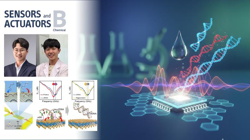
씻어서 다시 쓸 수 있는 저렴한 센서를 이용한 액체 생검 기술이 개발됐다. 고가의 액체 생검 비용을 낮출 수 있게 됐다. UNIST 전기전자공학과 김명수 교수팀은 KAIST 신우정 교수팀, 연세대학교 강주훈 교수팀과 공동으로 이황화몰리브덴(MoS2)과 고주파(RF)를 이용해 재사용 가능한 고감도 액체 생검 센서를 개발했다고 12일 밝혔다. 액체 생검은 실제 조직을 떼어내지 않고도 혈액이나 체액 속에 떠다니는 DNA 조각을 감지해 암을 찾아내는 기술이다. 하지만 기존 검사법은 감지 센서가 일회용이거나 센서 제작 비용이 커 비용 부담이 있었다. 연구팀이 개발한 이황화몰리브덴 센서는 특수 용액에 씻어내기만 하면, 5회 재사용할 수 있다. 제작도 쉬워 공정 비용도 저렴하다. 이황화몰리브덴 잉크를 기판에 발라 회전시킨 뒤 잉크 속 용매를 날려버리기만 하면 된다. 진단은 센서에 환자 체액을 떨어뜨린 뒤 고주파(RF)를 쏘아 반응을 살피는 방식인데, 표적 DNA가 센서에 달라붙을 때 발생하는 유전율과 저항의 변화가 고주파 신호의 공진 주파수를 이동시키는 원리다. 개발된 센서는 기존 유전자 분석 기술이 놓치기 쉬웠던 '단일 가닥 DNA'만을 검출해낸다. 단일 가닥 DNA는 말기 암이나 림프절 전이 환자에게서 고농도로 발견되는 바이오마커다. 일반적으로 DNA는 단일 가닥이 서로 마주 보고 결합한 이중 나선 가닥 형태로 존재한다. 실험에서 이 센서는 암 진단 지표인 'AluSx1' 유전자 DNA 조각을 154.67nM (나노몰)의 매우 낮은 농도까지 정확하게 검출해냈다. [연구그림] 재사용 할 수 있는 액체 생검 센서의 구조와 작동 및 재생 과정 한편, 센서를 세척 하는 특수 용액에는 상보 염기가 들어가 있다. DNA의 이중 나선은 염기라는 분자가 서로 마주 보고 결합해 생긴 구조인데, 서로 짝을 이룰 수 있는 조합, 즉 상보 조합이 정해져 있다. 센서 표면에 붙어 있던 단일 가닥 DNA가 세척액 속의 짝을 만나 결합하면서 이중 나선이 완성되고, 이중 나선 DNA는 별도 처리 없이도 센서에서 저절로 떨어진다. 이번 연구는 김명수 교수와 신우정 교수가 교신저자로, UNIST 이승찬 연구원과 KAIST 최은호 연구원이 제1저자로 주도했다. 공동 연구팀은 “암 전이와 밀접한 단일 가닥 DNA를 저비용으로 검출할 수 있게 돼, 향후 실제 임상에서 암전이 조기 진단과 예후 모니터링 비용을 획기적으로 낮출 수 있을 것”이라며 “병원을 넘어 가정에서도 손쉽게 암 예후를 관리할 수 있는 자가 진단 기기와 스마트 헬스케어 시스템으로 발전시켜 나갈 계획”이라고 말했다. 이 연구성과는 한국연구재단 개인기초연구(신진연구) 국가아젠다 기초연구, 기초연구실지원사업, BRIDGE융합연구개발사업, 정보통신기획평가원(IITP)의 지역지능화혁신인재양성사업의 지원으로 수행되었으며, 센서 분야의 국제학술지인 ‘센서 앤 액추에이터 B: 케미컬(Sensors and Actuators B: Chemical)’에 1월 22일에 온라인 게재됐다.

원자력공학과, ‘원자력 안전규제라운드테이블’ 개최

Research 2026년 09월 02일 수요일

New Process Shields 2D Semiconductors from Fabrication Residue

Abstract Achieving the theoretical performance of 2D molybdenum disulfide (MoS2) electronics is currently bottlenecked by interfacial contamination derived from lithographic processing. A critical, yet often overlooked, mechanism is the interaction between photoresist (PR) and plasma, which chemically alters the interface. In this work, we elucidate the atomistic origin of this degradation: theoretical calculations based on molecular dynamics (MD) and density functional theory (DFT) reveal that plasma exposure functionalizes the PR with oxygen, drastically increasing its adsorption energy on the MoS2 surface from −1.15 to −2.36 eV. This doubling of adsorption energy creates thermodynamically stable, hardened residues that resist conventional removal methods. To overcome this fundamental limitation, we introduce a universal prevention-first strategy: Sacrificial Metal Mask Lithography. By utilizing a sacrificial layer to physically isolate the channel, we shield the MoS2 from reactive plasma species, preventing the formation of hardened residue entirely. This strategy results in a ten-fold reduction in contact resistance (RC) from 2.59 × 10⁶ Ω·µm to 2.58 × 10⁵ Ω·µm and an order-of-magnitude enhancement in on-current. Crucially, we demonstrate the universality of this method by successfully applying it to top-gated transistor arrays, electron-beam lithography (EBL), and atomic layer deposition (ALD)-synthesized films. Two-dimensional (2D) semiconductors, such as molybdenum disulfide (MoS2) hold promise for smaller, thinner electronics, but their extreme thinness also makes them particularly vulnerable to contamination during fabrication. Even small amounts of residue can interfere with electrical performance. A research team, led by Professor Myung-Soo Kim of the Department of Electrical Engineering and Professor Byoung Jo Kim of the Graduate School of Semiconductor Materials and Devices Engineering at UNIST, has developed a fabrication method that protects MoS2 from photoresist (PR) residue. The approach uses a thin, removable metal layer to keep the residue from reaching the semiconductor surface. PR is a light-sensitive material used to pattern circuits during semiconductor fabrication. When exposed to plasma, however, it can leave residue on MoS2 that conventional solvents struggle to remove. More aggressive cleaning can damage or even detach the atomically thin material from its substrate. Rather than removing the residue after it forms, the researchers prevent it from reaching the MoS2 in the first place. They place a 5-nanometer-thick metal layer over the semiconductor before patterning. Once fabrication is complete, the metal is dissolved, carrying the accumulated residue with it. Transistors made with the new process had a contact resistance of 2.58 × 10⁵ Ω·μm, about one-tenth that of devices made conventionally. Their on-current, or the current flowing when the transistor is switched on, increased by roughly tenfold. The researchers also found no clear damage to the crystal structure of MoS2 after the metal layer was removed. The team also uncovered why the residue is so difficult to remove. Molecular-level calculations showed that plasma exposure introduces oxygen into the PR, changing its chemistry and causing it to bind much more strongly to MoS2. The calculated adsorption energy shifted from −1.15 to −2.36 eV, roughly doubling the strength of the interaction. “This process can be used not only with conventional semiconductor patterning, but also with electron-beam lithography for finer features,” said Dahyun Kim, first author of the study. “We also found that it works with MoS2 produced by different synthesis methods.” The researchers tested the method with top-gated transistor arrays, electron-beam lithography, and MoS2 films grown by atomic layer deposition, showing that it can be used across different device structures and fabrication methods. “MoS2 is a promising material for making semiconductor devices, such as transistors smaller and thinner,” said Professor Myung-Soo Kim. “By addressing process contamination that has limited device performance, this work could help advance highly integrated logic and memory devices based on 2D semiconductors.” The study was published online in Small on August 11, 2026. The research was supported by the Ministry of Science and ICT (MSIT), National Research Foundation of Korea (NRF), Institute of Information & Communications Technology Planning & Evaluation (IITP), InnoCORE program, Ministry of Trade, Industry and Energy (MOTIE), and Korea Institute for Advancement of Technology (KIAT). Journal Reference Dahyeon Kim, Yanfeng Zhao, Sungyeon Kim, et al ., “Preventing Plasma-Induced Resist Hardening in Molybdenum Disulfide Transistors via Sacrificial Metal Mask Lithography,” Small, (2026).

원자력공학과, ‘원자력 안전규제라운드테이블’ 개최

Research 2026년 09월 01일 화요일

Rethinking What Matters

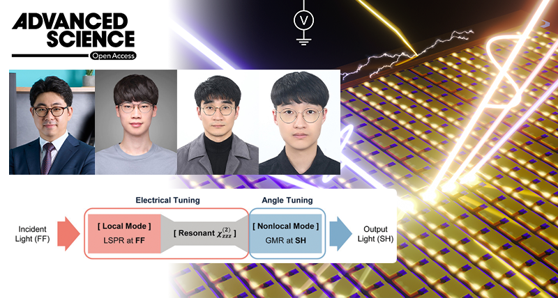
《Editor's Note: What does it take to make something work better? The answer may be to pare back what is unnecessary, rethink how existing parts are arranged, find another route around a constraint, or widen the frame of the problem itself. This month's UNIST research offers answers in many forms—from leaner AI systems and redesigned material structures to an unexpected route for electron transfer and a broader view of cancer drug resistance. Some of those answers run counter to what we might expect. 》 Less Can Be Enough “How much does AI really need?” AI has spent years scaling up. But recent UNIST research asks a different question—how much can be taken away while keeping what matters? At ACL 2026, researchers introduced GMoE, an architecture that shares experts across layers rather than repeatedly storing similar ones. It cut model parameters by about 63 percent, from 549 million to 204 million, while average accuracy remained virtually unchanged—39.51 percent, compared with 39.55 percent for the baseline. The next target was data. Presented at ICML 2026, CSOR removes redundant training images while preserving meaningful variation within each identity. Using roughly half the original dataset, models retained more than 95 percent of full-data performance in re-identification (ReID) tasks. A third study moved to hardware. An automated design framework for logic-in-memory (LiM) computing optimized the placement and routing of computing elements, cutting computation cycles by 19.6 percent under area constraints. ■ GMoE—Expert Sharing for Smaller AI Models (ACL 2026) ■ CSOR—Less Training Data for ReID AI (ICML 2026 ) ■ LiM—Smarter Chip Design (IEEE TCAD) Arrangement Matters “In materials, where can matter as much as what.” More iron, less corrosion. Iron (Fe) is one of magnesium's most damaging impurities, yet UNIST researchers produced a Mg alloy containing more than six times as much Fe as ultra-high-purity Mg—and it still corroded more slowly. Instead of removing the impurity, the team added scandium (Sc) to form core–shell particles that isolate Fe-rich regions from the surrounding Mg. The corrosion rate fell from 22.2 to 0.38 millimeters per year, nearly a 60-fold reduction. At the molecular scale, thermal annealing changed the packing of an organic semiconductor, more than tripling its absorption dissymmetry and even reversing its preferred handedness of circularly polarized light (CPL). The resulting near-infrared (NIR) photodetector achieved a dissymmetry factor of 0.1 at 850 nanometers. The scale shifts again in perovskite solar cells (PSCs). The same high-efficiency formulation crystallized differently depending on the buried interface beneath it. Tailoring the chloride chemistry to the inverted architecture produced a device with 26.3 percent efficiency and a fill factor (FF) of up to 86.8 percent. ■ Mg Alloy—Shielding Fe to Slow Corrosion (Science Advances) ■ NIR Photodetector—Turning Molecular Packing (Advanced Science) ■ PSCs—Why Architecture Changes Performance (Joule) Another Way Through “How spin opens a new route for electron transfer.” Conventional energetics suggested that electron transfer should be unfavorable. Yet in manganese (Mn)-doped quantum dots (QDs), spin-exchange interactions enabled transfer more than ten times faster than in undoped QDs. The mechanism could help capture energetic hot electrons before their excess energy dissipates—a longstanding challenge in photocatalysis and solar-energy conversion. ■ Hot Electrons—Spin-Enabled Transfer (Nature Communications) Beyond the Tumor “The cells helping cancer resist treatment.” Some of the cells helping breast cancer resist treatment are not part of the tumor at all. UNIST researchers found that nearby fat cells can become cancer-associated adipocytes, which release complement factor D and activate survival signaling in cancer cells. In mouse models, disrupting this TRAP1-driven communication improved the response to chemotherapy, pointing to surrounding adipocytes as potential therapeutic targets alongside the tumor itself. ■ Breast Cancer—How Nearby Fat Cells Drive Drug Resistance (STTT) Explore the latest issue and follow 『The UNIST Brief』 on LinkedIn to stay updated. Subscribe via LinkedIn

원자력공학과, ‘원자력 안전규제라운드테이블’ 개최

Research 2026년 08월 11일 화요일

Adaptive Wireless Charging for Implantable Medical Devices

Abstract This paper presents a wireless power transfer (WPT) system that maintains high efficiency and low output voltage ripple under large variations in coupling and load conditions. To address these variations, the proposed system employs an adaptive mode switching scheme with coupling-insensitive sensing. This is implemented using a fixed-reference sensor topology with filtered integrated sensor outputs and synchronization of RX 0X-to-1X transitions with TX 0X-to-1X mode transitions. For stable output regulation, a voltage-racing hysteretic controller is introduced to achieve low output voltage ripple, which is difficult to obtain with conventional analog feedback- or comparator-based hysteretic controllers. In addition, an on-chip load detector enables automatic detection of heavy- and light-load conditions. Fabricated in a 0.18- μ m BCD process, the proposed system was measured with coil distances from 7 to 20 mm, corresponding to coupling coefficient (k) variations from 0.42 to 0.08. The system supports an output power range from 2.6 mW to 147 mW while achieving a low ripple voltage of 18 mV and achieves a peak end-to-end efficiency of 69.1%. Implantable medical devices must continue operating reliably despite the body's constant movement—from walking and breathing to simply changing position during sleep. But those everyday movements can disrupt wireless charging by altering the alignment between the external charger and the implanted device. Researchers at UNIST have developed a wireless power transfer system that adapts to changes in body movement and device power demand. By maintaining stable power delivery while reducing unnecessary energy loss and heat generation, the system could make long-term wireless powering of implantable medical devices more practical. Many implantable medical devices alternate between active treatment and standby modes, causing their power requirements to change over time. At the same time, body movement can shift the distance or alignment between the transmitter and receiver coils, reducing wireless charging efficiency. Together, these challenges make it difficult to deliver stable power when and where it is needed. Led by Professor Franklin Bien of the Department of Electrical Engineering, the team designed the system to distinguish changes in device power demand from changes in coil alignment caused by body movement. Rather than relying solely on signal strength, it detects characteristic changes in communication between the transmitter and receiver, allowing it to switch reliably between high- and low-power modes as charging conditions change. The researchers also developed a new Voltage-Racing Hysteretic Controller (VRHC) to stabilize the receiver's output voltage. Instead of comparing voltages directly, the new controller detects voltage changes by measuring tiny differences in signal propagation time within the circuit. This allows it to respond more quickly and keep the output voltage remarkably stable. In laboratory tests, the system remained stable across transmission distances ranging from 7 mm to 20 mm. Even when the implanted device's operating current increased sharply from 6 mA to 16 mA, it maintained a constant 3.3 V output with a voltage ripple of only 18 mV. The system achieved a peak end-to-end power transfer efficiency of 69.1%, representing an improvement of up to 51.3 percentage points over a comparable design without the adaptive mode-switching technology. “Wireless charging systems need to adapt as conditions change, whether because a patient moves or a device's power demand shifts,” said Professor Bien. "By continuously adjusting power delivery in real time, our system improves both efficiency and stability. We hope it will help make implantable medical devices more practical for long-term use." The study was co-first authored by Sungmin Shin and Seongbin Kwon of UNIST. The research was supported by the Ministry of Science and ICT (MSIT) and the Institute for Information & Communications Technology Planning & Evaluation (IITP), and published in IEEE Transactions on Circuits and Systems I: Regular Papers (IEEE TCAS-I) on June 19, 2026. Journal Reference Sungmin Shin, Seongbin Kwon, Kiju Lee, et al ., "A Wireless Power Transfer System With Adaptive Mode-Switching Insensitive to Coupling Variations Achieving Low Ripple and High Efficiency," IEEE TCAS-I, (2026).

원자력공학과, ‘원자력 안전규제라운드테이블’ 개최

Research 2026년 08월 06일 목요일

Smarter Design Method Improves Efficiency of In-Memory Computing Chips

Abstract Data-centric applications continue to be limited by the memory wall. Logic-in-Memory (LiM) architectures based on non-volatile memories (NVMs), such as memristors, offer a promising solution by enabling in-memory computation and eliminating costly data movement. While several approaches leveraging memristor-aided logic (MAGIC) operations have been proposed, many fail to fully exploit the parallelism and spatial efficiency of memristor crossbars, especially under physical design constraints. In this paper, we propose a parallelism-driven, area-aware look-up table (LUT)-based mapping framework of arbitrary logic circuits into a memristor crossbar using MAGIC operations. We present a crossbar-aware floorplanning strategy that leverages topological LUT information to enable two-directional parallel computation (ie, HNOR and VNOR), thereby maximizing computational LUTs with minimal execution cycles. We formulate an integer linear programming (ILP) approach to define the placement of each LUT and its fanin locations, improving routability while preserving parallelism. Moreover, we introduce our novel A∗-search-based fan-in routing method with Hanan grid that fully utilizes the aligned fans and intermediate results. Experimental results demonstrate that the proposed framework achieves maximum parallelism and crossbar utilization, thereby reducing cycle counts by 19.6% and ensuring that all benchmarks map successfully under strict area constraints. We also confirm the scalability and practical applicability of the proposed framework for large-scale logic mapping in memristor-based LiM systems. Modern computing is increasingly limited not by processing speed, but by the time and energy required to move data between memory and processors. Researchers at UNIST have developed an automated design framework that addresses this challenge by making logic-in-memory (LiM) chips more efficient. Led by Professor Heechun Park of the Department of Electrical Engineering, the team designed a framework that automatically optimizes the placement of logic circuits and data pathways in memristor-based LiM architectures. By enabling more operations to run simultaneously while making better use of limited chip area, the approach reduced the number of computation cycles by nearly 20% compared with existing state-of-the-art methods. Unlike conventional computer chips, LiM architectures perform computation directly where data are stored, reducing costly data movement between memory and processors. This approach helps overcome the memory wall where data transfer limits overall computing performance. The framework determines where computations are performed within a memristor crossbar array and how intermediate results move to the next operation. Unlike previous approaches, it enables computations to proceed in both the horizontal and vertical directions, allowing more operations to run simultaneously while making better use of the available chip area. The framework also reorganizes intermediate data during computation, freeing unused memory cells and reducing wasted space. It then identifies efficient routes for transferring intermediate results between computational blocks, preserving parallel execution even under tight area constraints. In benchmark evaluations, chips designed using the new framework required 19.6% fewer computation cycles than those designed using existing approaches. The framework also successfully mapped every benchmark circuit, including designs that previous methods could not accommodate under the same area constraints, suggesting it can scale to larger LiM systems. “The performance of LiM computing depends not only on the memory device itself, but also on how computations are organized within the array,” said Professor Park. "By arranging operations to maximize parallel execution, our framework improves efficiency while remaning practical under realistic area constraints." The research was conducted by Ikkyum Kim and Minhong Kim as first and second authors, respectively, with Professor Heechun Park serving as the corresponding author. The findings were published online in IEEE Transactions on Computer-Aided Design of Integrated Circuits and Systems (IEEE TCAD) on June 2, 2026. The research was supported by the National Research Foundation of Korea (NRF) and the Institute of Information & Communications Technology Planning & Evaluation (IITP). The EDA tool was supported by the IC Design Education Center (IDEC). Journal Reference Ikkyum Kim, Minhong Kim, and Heechun Park, “A Parallelism-Driven, Area-Aware Technology Mapping Framework for Memristive Logic-in-Memory,” IEEE TCAD , (2026).

원자력공학과, ‘원자력 안전규제라운드테이블’ 개최

Research 2026년 08월 03일 월요일

Solution-Processed Semiconductor Enables High-Performance RF Switches for 6G and Satellite Communications

Abstract Next-generation 6G communication requires radio-frequency components capable of operating above 100 GHz with low loss, high isolation, and zero static power—requirements that challenge complementary metal-oxide-semiconductor (CMOS) and microelectromechanical systems (MEMS) technologies. Here, we report transfer-free, large-area millimeter-wave (mmWave) switches based on solution-processed MoS2. While solution-processed 2D materials are often viewed as inferior to their crystalline counterparts due to high defect densities, we demonstrate that their edge-rich morphology is, in fact, a performance enabler. These edge defects act as intrinsic templates that confine Cu-filament pathways, enabling rapid (76 ns) and low-energy switching (1.57 nJ) with > 2000 cycles and uniform zero static-power operation, as corroborated by Kelvin probe force microscopy, conductive atomic force microscopy and low-temperature studies. The resulting switches achieve an low insertion loss ( < 0.1 dB) and high isolation ( > 35 dB) at 67 GHz. Notably, they exhibit a switching figure-of-merit (RON·COFF) of ~ 0.8 fs (fco ~ 187 THz), surpassing previously reported 2D switches. Importantly, by adopting an inverse-state operational scheme in a SHUNT architecture, we mitigate self-switching and achieve improved power handling (P0.1dB > 10 dBm) and linearity (IIP3 > 42.1 dBm). Finally, we demonstrate the platform's circuit-level viability by integrating the switches into a true-time-delay and hybrid-coupled phase shifters targeting 30 GHz mmWave applications. Researchers at UNIST have developed a high-performance radio-frequency (RF) switch using a solution-processed two-dimensional (2D) semiconductor, demonstrating stable operation at frequencies up to 67 GHz while consuming no static power. The technology could support future 6G wireless networks, satellite communications, radar systems, and other high-frequency communication platforms that demand compact, energy-efficient components. Led by Professor Myungsoo Kim of the Department of Electrical Engineering, the team fabricated the device using a thin film of solution-processed molybdenum disulfide (MoS2). Unlike conventional fabrication methods that require 2D semiconductor films to be grown and transferred onto a substrate, the new approach forms the semiconductor layer directly from a liquid precursor, simplifying manufacturing and making large-area production more practical. RF switches are fundamental components in wireless communication systems. They control the flow of high-frequency signals in smartphones, wireless base stations, satellite communications, radar systems, and autonomous vehicles. As communication technologies move toward the millimeter-wave frequencies required for future 6G and space communications, RF switches must transmit signals with minimal loss, effectively block unwanted leakage, and operate with very low power consumption. The newly developed switch achieved all three. Operating at 67 GHz, it recorded an insertion loss below 0.1 dB and signal isolation greater than 35 dB, allowing nearly all of the incoming signal to pass while suppressing signal leakage to less than 0.03%. The device also requires no standby power. Once switched on or off, it maintains its operating state even after power is removed, reducing unnecessary energy consumption. The researchers attribute the device's durability to the characteristics of the solution-processed MoS2 film. During fabrication, naturally occurring sulfur vacuums help guide the movement of copper ions that create the conductive pathways responsible for switching. Rather than reducing performance, these defects stabilize the switching process. Devices fabricated using solution-processed films continued to operate reliably after more than 2,000 switching cycles, whereas comparable devices fabricated from mechanically exfoliated MoS2 showed a lifetime of only about 100 cycles. To evaluate its practical potential, the team integrated the switch into communication circuits used for high-frequency signal control, including a transmit/receive switch and a beam-steering phase shifter. Both operated successfully, demonstrating that the technology can be incorporated into circuits used in satellite communications, radar, defense systems, and future wireless networks. Beam-steering phase shifters electronically direct radio waves without physically moving the antenna, enabling fast and precise tracking of moving targets such as satellites and drones. “By using solution-processed 2D semiconductor materials, we developed an RF switch that combines low signal loss with excellent isolation in the millimeter-wave band without requiring complex transfer processes,” said Professor Kim. “Because the switch retains its operating state even when power is removed, it consumes no standby power and could contribute to smaller, more energy-efficient communication systems for 6G, satellite communications, radar, and defense applications.” The findings were published online in Nature Communications on June 18, 2026. The research was supported by the National Research Foundation of Korea (NRF) and the Institute of Information & Communications Technology Planning & Evaluation (IITP), including the Space-K BIG Project and the InnoCORE Program of the Ministry of Science and ICT (MSIT). Journal Reference Changwoo Pyo, Sungmoon Park, Seungchan Lee, et al ., "Sub-femtosecond figure-of-merit millimeter-wave switches via solution-processed MoS2 for 6G radio-frequency front-ends," Nat. Commun ., (2026).

원자력공학과, ‘원자력 안전규제라운드테이블’ 개최

Research 2026년 07월 14일 화요일

New Wearable Patch Combines Multimodal Sensing with On-Chip AI

Abstract A proposed chest patch device and its interface IC are configured to allow detection of multi-domain signals in the form of optical, electrical, acoustic, and chemical signals at a single body spot. The IC integrates on-chip classification capabilities for cardiovascular diseases (CVDs) based on photo-plethysmogram (PPG) and electrocardiogram (ECG), along with hazardous gas analysis. For low-power multimodal sensing, an ECG R-peak_triggered PPG window (RPT-PW) is proposed as an inter-sensor scheme to reduce activity on the PPG channel, which is the dominant energy consumer. Additionally, the PPG and ECG readout channels incorporate analog peak detection to enable normalized on-chip extraction of pulse arrival time (PAT) and RR interval (RRI). For minimal computation and communication power, a multi-domain convolutional neural network (MD-CNN) processes both analog and digital inputs, and a reconfigurable analog ternary/binarized neural network (a-TNN/BNN) provides additional computation capability for multi-domain applications. The IC was fabricated in an 180-nm BCD process and integrated into a chest patch device prototype with an in-house adhesive meta patch. The RPT-PW demonstrated adaptive operation with an effective LED duty cycle (EDC) as low as 0.02%. The on-chip computation achieved average sensitivity and specificity of 90.87%/95.38% for three-label hypertension, 92.80%/96.36% for three-label arrhythmia, and 92.46%/97.50% for four-label gas mixture classification. Continuous wearable monitoring often requires transmitting large volumes of sensor data to external devices for analysis, increasing power consumption and limiting operating time. A joint research team, led by Professor Jae Joon Kim of Electrical Engineering and Professor Hoon Eui Jeong of Mechanical Engineering, has developed a wearable chest patch that analyzes physiological and environmental signals directly on the device, reducing both communication and sensing power while enabling continuous real-time monitoring. The wearable integrates optical, electrical, acoustic, and chemical sensing into a single device capable of simultaneously monitoring cardiovascular signals and hazardous gases. Rather than transmitting raw sensor data, it processes the information using an on-chip AI processor and sends only the analysis results via Bluetooth. This reduces communication overhead while allowing multiple users to be monitored remotely. To extend battery life, the researchers introduced an adaptive sensing scheme that selectively activates the optical sensor—the most power-intensive component of the device. By synchronizing optical measurements with ECG signals, the system reduced power consumption in the optical sensing channel by approximately 83%, enabling longer operation on a single charge. The device achieved more than 90% sensitivity and specificity in classifying hypertension and cardiac arrhythmias. It also classified hazardous gas mixtures with 92.46% accuracy, demonstrating its ability to monitor both physiological conditions and environmental hazards using a single wearable platform. The chest patch incorporates a microstructured adhesive interface that conforms securely to rough skin while allowing clean removal without leaving residue, making it better suited for long-term wear. “This work brings multimodal sensing and AI inference together on a single wearable platform,” said Professor Kim. “By processing information directly on the device, the system reduces communication demands while enabling continuous monitoring of both health conditions and environmental hazards.” The study has been participated by Sanghyeon Cho and Hyunjoong Kim as co-first authors. Their findings will appear in the July 2026 issue of the IEEE Journal of Solid-State Circuits (JSSC) , one of the leading journals in integrated circuit design. The technology has been licensed to Anvix Lab, a startup co-founded by the research team, which is pursuing commercialization of next-generation bioelectronic patch platform based on on-chip AI. The research was supported by the Ministry of Trade, Industry and Energy (MOTIE), the Ministry of Education (ME), and the Ministry of Science and ICT (MSIT). Journal Reference Sanghyeon Cho, Hyunjoong Kim, Dong Kwan Kang, et. al., “An Energy-Efficient Chest Patch Interface With Inter-Sensor PPG Windowing and Multi-Domain On-Chip Analog Computing,” JSSC , (2026).

원자력공학과, ‘원자력 안전규제라운드테이블’ 개최

Research 2026년 07월 02일 목요일

New Semiconductor Device Brings Communication and AI Computing onto a Single Chip

Abstract Next-generation 6G communication systems necessitate hardware that simultaneously manages high-frequency signal routing and massive matrix-level computations under extreme constraints. However, conventional digital architectures suffer from high power dissipation and area overhead. Here, we report an oxidized molybdenum disulfide (MoS2)-based memristive platform that integrates nonvolatile radio-frequency (RF) switching and energy-efficient vector–matrix multiplication. By implementing a controlled thermal oxidation process, we achieve stable resistive switching with low switching energy and zero-static power consumption, while maintaining a high cutoff frequency of 33.2 THz, outperforming existing phase-change and microelectromechanical systems (MEMS) technologies. Using system-level simulations, we demonstrate the robustness of this hardware through successful 1024-quadrature amplitude modulation (1024-QAM) demodulation, spectral analysis, and multiple-input multiple-output (MIMO) signal reconstruction, even when accounting for intrinsic device non-idealities. This monolithic integration of high-frequency switching and analog computing provides a scalable solution for energy-efficient deployment of intelligent wireless systems. Future 6G networks and satellite communication systems will require hardware that can process growing amounts of data while operating under strict power and space constraints. Professor Myungsoo Kim and his research team from the Department of Electrical Engineering at UNIST introduced a new semiconductor device that combines high-frequency signal switching and computation on a single platform, offering a more compact and energy-efficient approach to next-generation wireless systems. At the heart of the platform is a multifunctional memristor based on oxidized molybdenum disulfide (MoS2), a two-dimensional semiconductor. The device functions as both a radio-frequency (RF) switch and hardware for in-memory matrix operations, bringing communication and computation onto a single chip. Conventional communication systems typically separate these functions, requiring signals to move between switching circuits and processors. This data movement increases power consumption, processing delays, and chip size. By integrating both functions into a single device, the new platform simplifies signal processing while improving energy efficiency. The memristor also operates without standby power. Once switched between its ON and OFF states, it retains that state even after power is removed, making it particularly well suited to energy-constrained applications such as satellite communications and future 6G infrastructure. The device demonstrated a switching energy of just 140 picojoules per operation and switching power below one milliwatt. It maintained stable operation for more than 40,000 seconds and over 1,000 switching cycles, while achieving a calculated cutoff frequency of 33.2 THz. Experimental measurements verified high-frequency switching up to 67 GHz. To evaluate its computing capability, the researchers performed system-level simulations of wireless communication tasks. The device successfully carried out 1024-quadrature amplitude modulation (1024-QAM) demodulation and multiple-input multiple-output (MIMO) signal reconstruction, demonstrating that a single hardware platform can efficiently support both communication and signal processing. "Commercial RF switches continuously consume standby power and often suffer signal loss at high frequencies," said Juhyo Son, the study's first author. "Our device addresses these limitations while remaining competitive with existing phase-change memory and MEMS technologies in energy efficiency, operating speed, and scalability." Professor Kim added, "Our study demonstrates that oxidized MoS₂ memristors can function not only as high-performance RF switches but also as hardware for the in-memory matrix operations required for next-generation wireless communications. By combining nonvolatile operation, low power consumption, and high-frequency performance, this platform could contribute to more compact and energy-efficient systems for satellite communications, radar, defense electronics, and future 6G RF front ends." The research was supported by the National Research Foundation of Korea (NRF) through the Ministry of Science and ICT (MSIT), the Institute for Information & Communications Technology Planning & Evaluation (IITP), the Space-K BIG Project, and a regional talent development program. The findings were published online in Advanced Functional Materials on June 6, 2026. Journal Reference Juho Son, Changwoo Pyo, Sungmoon Park, et al., “ Oxidized MoS2-Based Multifunctional Memristive Hardware for Energy-Efficient mmWave Signal Processing and In-Memory Matrix Multiplication ,” Adv. Funct. Mater., (2026).

원자력공학과, ‘원자력 안전규제라운드테이블’ 개최

News 2026년 06월 09일 화요일

UNIST Selected to Lead National Space-K BIG Project for Very Low Earth Orbit Satellites

UNIST has been selected to lead a major national research project aimed at developing core technologies for very low Earth orbit (VLEO) satellite platforms, reinforcing Korea's efforts to strengthen its space technology capabilities. The project is part of the 2026 Space-K BIG Project, an initiative of the Korea AeroSpace Administration (KASA) that designs leading university research centers to advance foundational space technologies while training the next generation of space professionals. Under the program, the Department of Electrical Engineering at UNIST will receive KRW 5.7 billion in government funding through December 2030. The project, led by Professor Gangil Byun from the Department of Electrical Engineering , brings together Professors Myungsoo Kim, Hoon Lee, Jinseok Park, Minho Choi, Dongyun Kam, Kawon Han, and Jaeyong Jeong in a multidisciplinary effort. Titled "Mission-Oriented Convergent Platform Technologies for Very Low Earth Orbit Satellites and Global Talent Development," the project will develop key technologies for future satellite missions, including space-qualified RF devices, AI semiconductors, and optoelectronic components. Researchers will also advance domestically developed commercial off-the-shelf (COTS) technologies for satellite applications and establish an integrated VLEO satellite platform for future mission deployment. Education and workforce development form another major component of the initiative. UNIST will collaborate with industry, government research institutes, and international partners to provide students with hands-on research experience through joint projects and specialized training, creating an integrated environment that connects education with advanced space research. “This project provides an important opportunity for UNIST to lead research on core technologies for very low Earth orbit satellites while cultivating globally competitive talent in space engineering,” said Professor Gangil Byun, the project's principal investigator. “By combining the expertise of our faculty with the innovative capabilities of our industry partners, we aim to deliver technologies that will contribute to the future growth of Korea’s space industry.”

원자력공학과, ‘원자력 안전규제라운드테이블’ 개최

Community 2026년 06월 05일 금요일

Professor Sung Whan Yoon Receives MSIT Commendation for Digital Talent Development

Professor Sung Whan Yoon of the Graduate School of Artificial Intelligence (AIGS) and Department of Electrical Engineering at UNIST has been honored with a Ministerial Commendation from the Ministry of Science and ICT (MSIT) for his contributions to digital talent development. The award recognizes his efforts to advance reliable AI technologies, while connecting AI education with real-world manufacturing challenges. A major challenge in applying AI to factories is the gap between the lab and the field. Data collected from actual equipment often differs from the data used to train a model. Changes in materials, machine conditions, operating methods, or data quality can all weaken model performance. In manufacturing, those errors can lead directly to production losses or safety risks. Professor Yoon has worked to address that problem through robust AI algorithms. Robust AI refers to machine learning systems that continue to perform reliably even when conditions change. Rather than pursuing high accuracy only under fixed conditions, his work focuses on AI that can make dependable decisions in real industrial environments. His research has also drawn international recognition. At the International Conference on Learning Representations (ICLR) 2025, one of the world’s leading AI conferences, his work on improving the stability of reinforcement learning models was selected for an oral presentation. Oral presentations at ICLR are typically reserved for roughly the top 2 percent of submitted papers. Reinforcement learning allows AI systems to improve decisions through trial and error. In manufacturing, it can help optimize equipment settings and production processes. But factories leave little room for unstable decisions, since one wrong choice can create cost and safety risks. Professor Yoon’s research showed how reinforcement learning models can become more stable under uncertain or changing field conditions, moving the technology closer to industrial use. Beyond research, Professor Yoon has also brought those advances into AI education for manufacturing professionals. Since joining UNIST, Professor Yoon has helped design and run AI programs for industry workers in Ulsan and the southeastern region. The programs are built around problems participants face in their own factories, turning actual production issues into hands-on AI projects. His team has applied reinforcement learning-based optimization methods to manufacturing and processing facilities. The work aims to improve equipment operations while maintaining process stability and safety. This link between AI training and workplace change was a key reason for the commendation. Professor Yoon currently serves as a project leader in the national AI Star Fellowship program. In partnership with SK Energy, he is developing core technologies for robust manufacturing AI that can be used in complex process industries, including petrochemicals. “High performance alone is not enough for AI to succeed in industry,” Professor Yoon said. “AI systems must remain stable even when conditions change. We will continue developing robust AI technologies and connecting them to manufacturing solutions and digital talent development.”

원자력공학과, ‘원자력 안전규제라운드테이블’ 개최

Research 2026년 06월 05일 금요일

New High-Efficiency Wireless Charging for Implantable Medical Devices

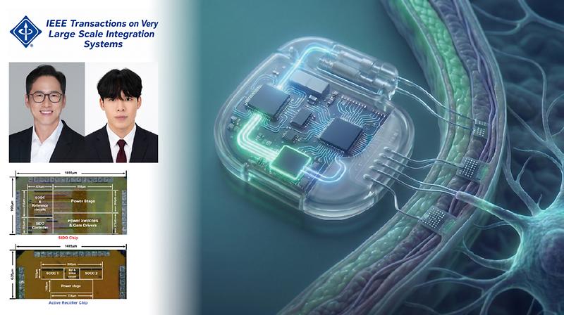
Abstract This article presents a single-input–dual-output (SIDO) wireless power transfer (WPT) system that maintains high link efficiency across both heavy and light load conditions. Conventional SIDO architectures employ a fixed matching network, which leads to significant efficiency degradation when the load changes. To address this limitation, the proposed system classifies the two outputs into heavy-load and light-load domains and employs dedicated matching networks optimized for each operating condition, thereby maximizing link efficiency during charging of either load. To minimize the power overhead of mode switching while enabling single-stage AC–DC regulation, a charging-phase controller, a full/half-window mode controller, and an adaptive window generator are employed. Furthermore, an active rectifier with a slowdown unit cell (SUC)-based on/off controller (SOOC) is proposed to improve power conversion efficiency (PCE). In addition, an early turn-on switching (ETS) is implemented to achieve higher PCE compared to conventional zero-voltage switching (ZVS). Fabricated in a 0.18- μ m BCD process, the system is implemented as two chips, a standalone rectifier for accurate PCE measurement and a SIDO integrating the same rectifier. The SIDO demonstrates stable full/half-window operation without multiple pulsing. Measured link efficiency reaches 94.4% at 3mA and 92.7% at 30mA at a coupling coefficient k = 0.2, confirming the effectiveness of the load-optimized matching. The rectifier achieves 94.5% peak PCE and maintains above 92.3% PCE across a 2.5–5.0V input range. A new wireless charging technology promises to enhance the safety and longevity of implantable medical devices, such as pacemakers and neural stimulators. Led by Professor Franklin Bien of the Department of Electrical Engineering, the research team developed a system that employs load-specific matching networks and adaptive control to optimize power delivery. Implantable devices often incorporate circuits with varying power demands—high-current circuits for stimulation and low-current circuits for data processing. Traditional wireless chargers rely on fixed configurations, which can lead to inefficiencies and heat buildup, potentially damaging surrounding tissue. The new system detects changes in load and switches between dedicated matching networks tailored for high and low power conditions, thereby optimizing energy transfer. Furthermore, the team improved the efficiency of the rectifier circuit that converts received alternating current (AC) into direct current (DC). By precisely controlling switching points during power conversion, they minimized energy loss and enhanced overall performance. Experimental results demonstrated a link efficiency of 94.4% at a low load of 3mA and 92.7% at a high load of 30mA. The active rectifier achieved a peak power conversion efficiency of up to 94.5%, maintaining above 92% even as input voltage varied from 2.5V to 5V. The research team anticipates that this technology will extend the operational lifespan of implantable devices, reducing the need for frequent surgical replacements and associated risks. It also holds promise for application in wearable electronics and compact Internet of Things (IoT) devices that require reliable, low-loss wireless power. The findings of this research were published online in the IEEE Transactions on Very Large Scale Integration (VLSI) Systems on April 29, 2026. The study has been s upported by the Ministry of Science and ICT (MSIT) and the Institute for Information & Communications Technology Planning & Evaluation (IITP). Journal Reference Sungmin Shin, Seongbin Kwon, Geonwoo Baek, et al ., “A Single-Input Dual-Output Wireless Power Transfer System With Load-Optimized Matching Network,” IEEE TVLSI. , (2026).

원자력공학과, ‘원자력 안전규제라운드테이블’ 개최

Research 2026년 06월 01일 월요일

Breakthrough Chameleon MXene Promises Advanced 6G Communication and Next-Gen Batteries

Abstract Device-level performance in MXenes is dictated by architecture—planar nanosheets are optimal for electromagnetic interference (EMI) shielding, while scrolled structures enhance ion transport for energy storage—particularly when morphology is programmed at synthesis. Whether such architectures can be deterministically encoded through precursor stoichiometry remains unresolved. Here, we demonstrate that precise carbon stoichiometry control in Ti3AlCxO2-x MAX phases tunes internal lattice strain and thereby directs the emergent MXene architecture. Carbon-rich precursors (x = 1.94) yield strain-relieved, high-crystalline nanosheets with metallic conductivity (∼23 300 S cm−1), enabling ultrathin films with record-high EMI shielding performances across 8 µm) and robust W-band retention after 5,000 bending cycles (r = 2.5 mm). In contrast, carbon-deficient precursors (x = 1.71) introduce lattice compression and oxygen substitution, triggering spontaneous scrolling upon delamination. The resulting nanoscrolls offer exceptional ion accessibility, achieving 657 F g−1 at 2 mV s−1 with 99.4% retention over 12 000 cycles. This stoichiometry-programmed approach establishes a synthesis-stage lever linking MAX chemistry to MXene architecture and function, enabling application-specific architecture design within established MAX/MXene synthesis and solution-processing workflows for next-generation electronics and energy storage. Researchers at UNIST have discovered a simple way to control MXene's structure by adjusting the carbon content in its precursor. This breakthrough enables the creation of tailored MXene materials optimized for high-frequency electromagnetic interference (EMI) shielding and rapid energy storage. MXene, a two-dimensional material composed of metal and carbon layers, is celebrated for its excellent electrical conductivity and adaptability. Its potential spans batteries, sensors, and flexible electronics. With the rise of 6G technology and advanced radar systems, shielding devices against high-frequency interference has become critical. At the same time, the demand for quick, reliable energy storage continues to grow. Led by Professor Soon-Yong Kwon from the Graduate School of Semiconductor Materials and Devices Engineering and Professor EunMi Choi from the Department of Electrical Engineering, the team showed that changing the carbon content in MAX precursors influences how MXene forms during synthesis. This control method results in two distinctly different structures. When using carbon-rich precursors, the process yields flat, highly crystalline nanosheets that exhibit excellent electrical conductivity, effective electromagnetic shielding at 100 GHz, and maintain flexibility and durability under repeated bending. Conversely, employing carbon-deficient precursors induces the spontaneous formation of nanoscrolls, which significantly enhance ion transport. These nanoscroll structures enable high-capacity energy storage, achieving a capacitance of 657 F/g and a cycle life exceeding 12,000 cycles. This work confirms that simple adjustments to precursor composition can produce MXene structures tailored for specific applications—flat sheets for shielding and scrolls for energy storage—within a streamlined process. First author Jaeeun Park explains, “We showed that flat MXene sheets are ideal for electromagnetic shielding, while scroll structures are better suited for energy storage. By controlling the precursor, we can design the material for different functions without changing the synthesis method.” Professor Kwon adds, "Last year, we enhanced MXene's conductivity and broadband shielding through nitrogen doping. Now, we've demonstrated how to design the material's shape from the start. The ultra-thin, flexible MXene performs well at 100 GHz and withstands bending, making it a promising lightweight, flexible shield for future 6G and radar systems." Supported by the Ministry of Science and ICT (MSIT) and the National Research Foundation of Korea (NRF), the study was published in Advanced Materials on May 18, 2026. Journal Reference Jaeeun Park, Ju-Hyoung Han, Yujin Chae, et al ., “Stoichiometry-Programmed MXenes via Precursor Engineering for High-Performance EMI Shielding and Energy Storage,” Adv. Mater ., (2026).

원자력공학과, ‘원자력 안전규제라운드테이블’ 개최

Research 2026년 05월 12일 화요일

Revolutionizing Semiconductor Design: AI Cuts Development Time from Months to Just One Day

Abstract Artificial Intelligence (AI) has been increasingly utilized across various fields, including communications, healthcare, and Computer-Aided Design (CAD). However, AI has shown relatively limited advances in analog and RF circuit design, which are critical for modern communication systems such as 5G due to their higher complexity and nonlinear characteristics. For example, the Inductor-Capacitor Voltage-Controlled Oscillator (LC-VCO) is a crucial component in frequency synthesizers, determining the performance of RF systems, including high data transmission rates and wide bandwidth. In fact, LC-VCO design is challenging due to the high parameter variability and complex interactions between design variables, making it challenging to optimize parameters to meet target specifications. Thus, this study proposes a comprehensive LC-VCO design methodology compatible across multiple process nodes and supports optimization down to the layout level. We use Reinforcement Learning (RL) to navigate the nonlinear design space efficiently for schematic optimization and apply an algorithm from Gradient Descent to optimize the design at the physical layout level. We highlight that the versatility of our methodology is demonstrated by producing optimized Figures of Merit (FoM) across various technology nodes and frequency ranges, showcasing its potential as a universal design tool accessible to all users. A team of researchers from UNIST and Kyungpook National University (KNU) has unveiled a pioneering AI system capable of completing the complex design of high-performance semiconductor circuits in just one day—an achievement that drastically reduces the traditional development timeline, which can take several months. Led by Professor Heein Yoon of UNIST’s Department of Electrical Engineering and Professor Taigon Song of KNU, the team developed an integrated AI platform that automates the entire process—from schematic design to physical chip layout. This breakthrough technology streamlines a typically multi-stage, resource-intensive task, offering faster, more efficient, and highly optimized circuit design solutions. The initial focus was on the design of the Inductor-Capacitor Voltage-Controlled Oscillator (LC-VCO), a critical component in 5G and emerging 6G communication systems. LC-VCOs generate the carrier signals essential for high-speed data transmission. Designing these circuits involves balancing numerous variables—such as inductor and transistor sizes—to minimize noise and power consumption. However, translating schematic designs into physical layouts often introduces parasitic effects that can impair performance. The new model integrates circuit schematic optimization with physical layout design, addressing these challenges holistically. During the schematic phase, reinforcement learning algorithms explore various parameter configurations to meet specific frequency and performance targets. Subsequently, in the layout phase, the system employs gradient descent methods to iteratively refine physical design parameters—such as wire widths and spacing—to enhance overall circuit performance. Gradient descent, a well-established optimization technique, incrementally adjusts design variables by following the gradient of the objective function toward an optimal solution. This integrated approach drastically accelerates the design process. Tasks that previously required up to 119 hours can now be completed in approximately 28.5 hours—reducing the overall time by over 76%. Moreover, the system’s adaptability across different semiconductor process nodes is enabled by transfer learning. Models trained on one technology node (e.g., 65nm) can be efficiently adapted to others (such as 40nm or 28nm), using just around 10% additional data. This AI-driven methodology not only shortens development cycles and reduces costs but also addresses the industry’s growing need for efficient design automation amid a global talent shortage. By ensuring high performance while minimizing manual effort, this technology is poised to significantly impact the production of next-generation communication and AI chips. The researchers anticipate expanding this framework beyond LC-VCOs to automate various analog and RF circuit designs, further accelerating innovation in semiconductor technology. The research was led by Sungjin Kim of UNIST and Hyunsoo Lee of KNU, who served as co-first authors, with additional contributions from Hong Seong-min of KNU. The findings of this research have been published online in the IEEE Transactions on Computer-Aided Design of Integrated Circuits and Systems (TCAD) on April 3, 2026. The study has been supported by the Ministry of Science and ICT (MSIT), the National Research Foundation of Korea (NRF), the Ministry of Education (BK21 Four), the Ministry of Trade, Industry and Energy (MOTIE), the Semiconductor Design Education Center (IDEC), Samsung Electronics, Axion Co., Ltd., and the Institute for Information & Communications Technology Planning & Evaluation (IITP). Journal Reference Sungjin Kim, Hyunsoo Lee, Seongmin Hong, et al., "A Framework of Automated LC-VCO Design with Physical Layout Based on Reinforcement Learning, IEEE TCAD, (2026).

전기전자공학과의 다양한 소식
을 전달드립니다.

전기전자공학과에서 진행중인
세미나 입니다.

View More

배너존